Osp
by:A-TECH
2020-09-09
Visual and electrical inspections are made all through the manufacturing course of to detect flaws. For instance, elements are sometimes misplaced on the board or shifted before final soldering. Other flaws are brought on by the applying of an excessive amount of solder paste, which can trigger extra solder to flow, or bridge, throughout two adjacent printed circuit paths.
The gap partitions for boards with two or more layers can be made conductive after which electroplated with copper to type plated-via holes. For multi-layer boards, these with three layers or extra, drilling sometimes produces a smear of the high temperature decomposition products of bonding agent in the laminate system. Before the holes may be plated through, this smear must be eliminated by a chemical de-smear process, or by plasma-etch. The de-smear process ensures that an excellent connection is made to the copper layers when the opening is plated through. On high reliability boards a course of called etch-again is carried out chemically with a potassium permanganate primarily based etchant or plasma.
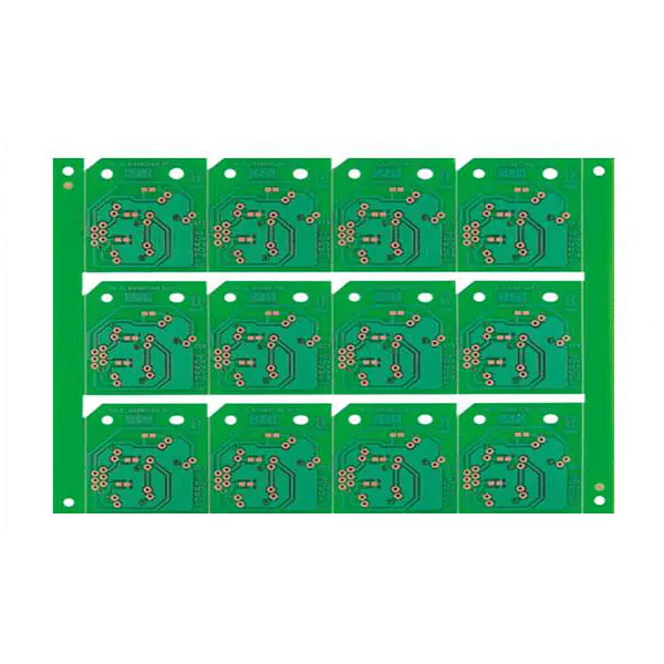
Each board has a singular perform for a selected product and must be designed to carry out that operate in the house allotted. Board designers use laptop-aided design methods with special software to format the circuit pattern on the board.
In 1903, a German inventor, Albert Hanson, described flat foil conductors laminated to an insulating board, in a number of layers. Thomas Edison experimented with chemical strategies of plating conductors onto linen paper in 1904. Arthur Berry in 1913 patented a print-and-etch method in the UK, and within the United States Max Schoop obtained a patent to flame-spray metallic onto a board via a patterned mask. Charles Ducas in 1927 patented a way of electroplating circuit patterns.
Heating the solder too quickly within the ultimate reflow process could cause a 'tombstone' impact the place one end of a part lifts up off the board and does not make contact. With surface mount expertise, the soldering is completed by passing the boards via another reflow course of, which causes the solder paste to soften and make the connection.
PCBs meant for extreme environments often have a conformal coating, which is applied by dipping or spraying after the parts have been soldered. The coat prevents corrosion and leakage currents or shorting due to condensation. The earliest conformal coats have been wax; fashionable conformal coats are often dips of dilute solutions of silicone rubber, polyurethane, acrylic, or epoxy. Another approach for making use of a conformal coating is for plastic to be sputtered onto the PCB in a vacuum chamber. The chief drawback of conformal coatings is that servicing of the board is rendered extremely troublesome.
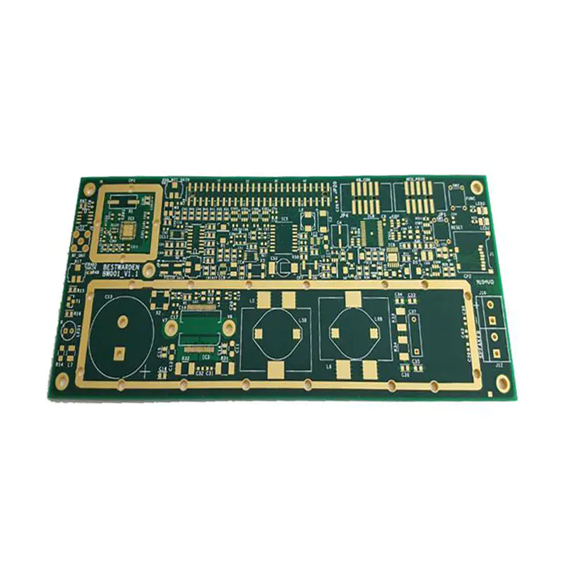
The spaces between electrical conducting paths are sometimes 0.04 inches (1.zero mm) or smaller. Pecht, 'Reliability Issues of No-Clean Flux Technology with Lead-free Solder Alloy for High Density Printed Circuit Boards', thirty eighth International Symposium on Microelectronics, pp. 367–375, Philadelphia, PA, September 25–29, 2005. A PCB as a design on a pc (left) and realized as a board meeting populated with elements (proper). The board is double sided, with by way of-gap plating, inexperienced solder resist and a white legend. Development of the strategies utilized in trendy printed circuit boards started early within the 20th century.
Custom message