Matters needing attention on PADS file transfer
by:A-TECH
2021-03-28
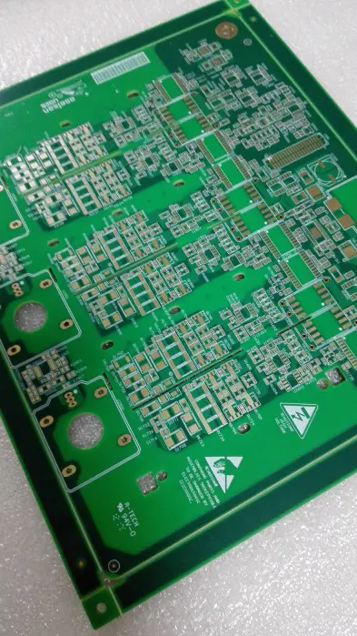
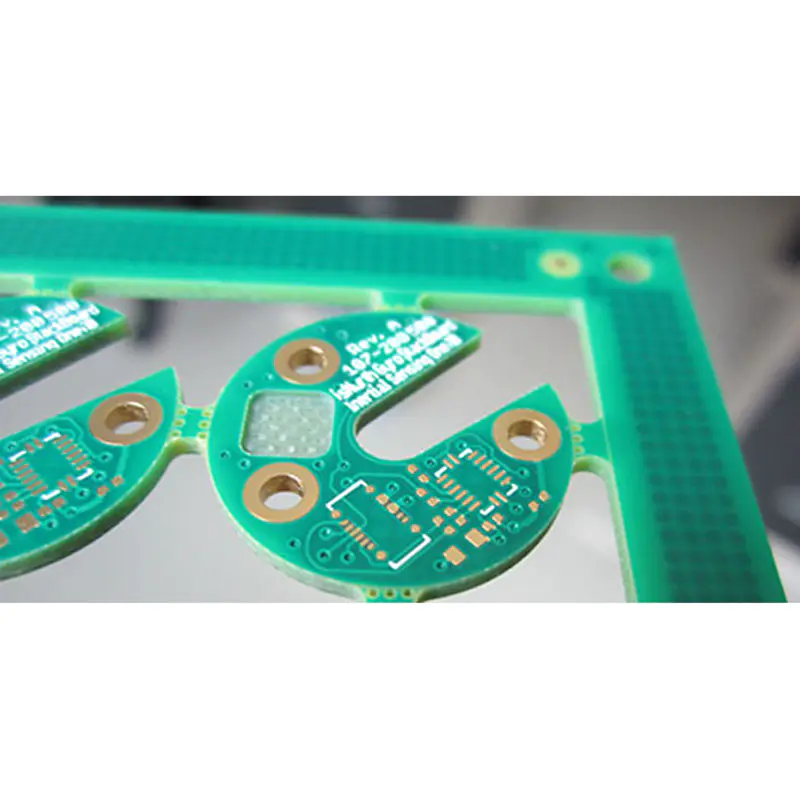
Due to different disputes between Pads files and gerber, after sorting out customer complaint records and engineering interview records, the areas that are prone to disputes are now unified: 1. As long as the options indicated by the arrow '1' in Figure 1 are ticked and If the color is marked, it will be transferred out. If the color is not marked and the color is black, it will not be turned. 2. As shown in the figure 1 arrow '2' refers to the layer according to the line, solder mask, character, hole map, drill belt Turn out one by one, (necessary layers, such as the circuit layer, please turn on, if the layer is turned off, it may not be turned out, or the display is black, do not turn to this layer. Please make special notes before placing orders for special layers.) 3 . Define the layer represented by the layer name in PADS/POWERPCB. Top: Top line Bottom: Bottom line SoldermaskTop: Top solder mask SoldermaskBottom: Bottom solder mask SilkscreenTop: Top silk screen SilkscreenBottom: Bottom silk screen. DrillDrawing: Hole diagram (general shape, hole symbol, hole position, attributes are all reflected in this picture) NCDrill: Drilling layer four-layer board, there will be an inner layer, for example, LAYER2 represents the second layer of the inner layer, and LAYER3 represents the first layer of the inner layer. Three floors. The six-layer board and so on.
Custom message