Introduce the Layer25 layer in PADS in detail
by:A-TECH
2021-03-18
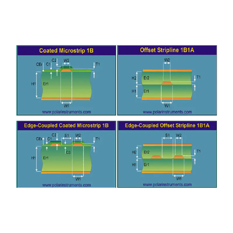
The Layer25 layer is only available for plug-in devices. It is only useful when producing negative films. Generally, the geber file will produce negative films only when the power layer is defined as CAM Plane (split/Mixe is also a positive film). This layer, the pins of this layer are easy to short-circuit when the negative film is output. There are two options for setting the power layer and ground layer in PowerPCB, CAMPlane and Split/Mixed. Split/Mixed is mainly used when multiple power sources or grounds share one layer, but it can also be used when there is only one power source and ground. Its main advantage is that the output diagram is consistent with the light drawing, which is easy to check. The CAM Plane is used for a single power supply or ground. This method is a negative output. Note that the 25th layer must be added when outputting. The 25th layer contains the ground electrical information, which mainly refers to the safety distance of the electrical layer pads being about 20 mils larger than the normal pads to ensure that there will be no signals connected to the ground after the metallized vias. This requires that each weld contains the 25th layer of information. We often ignore this problem when we build our own library. Alternative settings for Layer25: In the pad settings of PADS, there is an AntiPad setting. As long as this item can be enabled (select the pad type), the initial setting value of the pad is ordinary pad +24mil or 0.6mm, looking at the function and effect of this setting, it can replace the role of Layer25, and this setting feels more formal. It's just that, relatively speaking, Layer 25 has a long history of practice. Many people are used to it, and novices can try it. Another point is that you can use Layer25 to set this item when building components, while AntiPad needs to be set in the layout. The processing of vias is similar. You can add layer25 to vias or set vias. AntiPad. In general, whether you use Layer25 or Antipad, the ultimate goal is two: one is to prevent short circuits when metalizing the vias mentioned above; the other is to reduce the induced capacitance and inductance of the vias.
Custom message