Internal structure of PCB circuit board
by:A-TECH
2020-05-04
When a hardware engineer first contacts a multi-layer PCB, it is easy to look dizzy.
Ten layers and eight layers, the line is like a spider web.
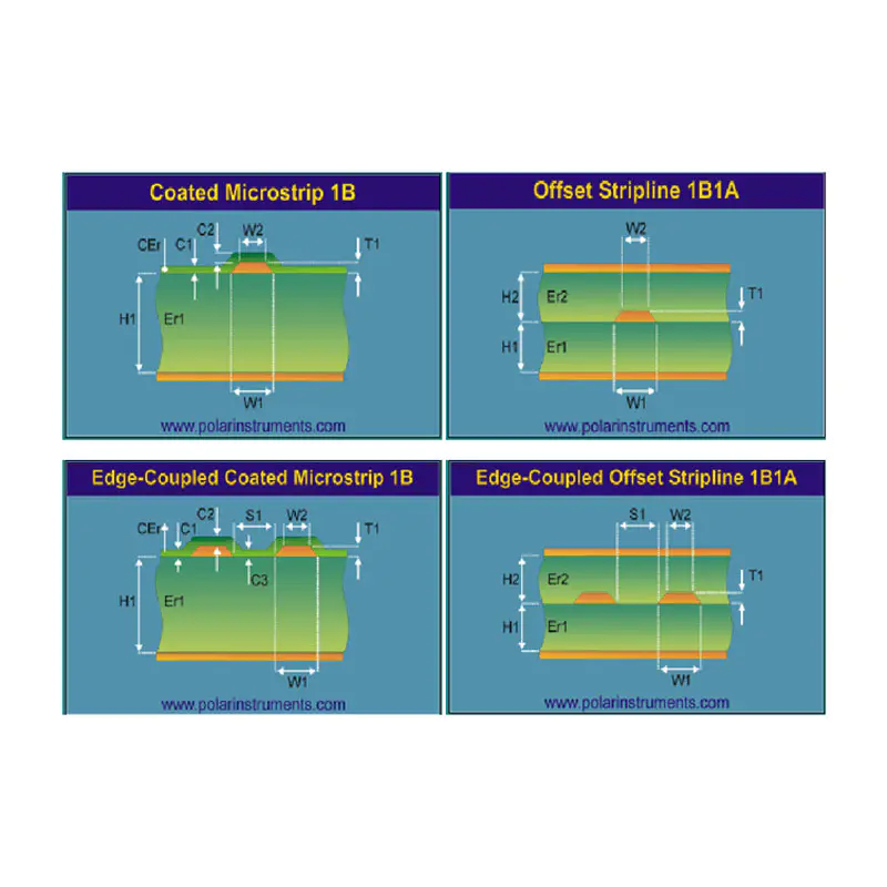
The editor drew several internal structure diagrams of multi-layer PCB circuit boards, and showed the internal structure of PCB diagrams of various laminated structures with three-dimensional graphics. Feel good, give me a compliment!
The circuit processing of multi-layer PCB is no different from that of single-layer and double-layer PCB. The biggest difference lies in the process of vias.
The lines are all etched, and the vias are all drilled and then plated with copper. Everyone who does hardware development knows this, so I won't go into details.
If you don't understand, you can look at the two articles before the smart headline. Articles on PCB technology-1PCB technology article-
2 Multi-layer circuit boards usually have through-plate, first-order plate, second-order plate and second-order laminated plate.
Higher-level boards such as third-order boards and any layer interconnection boards are usually used very little, and the price is expensive.
In general, 8-bit single chip microcomputer products use 2-layer through-hole plates;
32-bit MCU level intelligent hardware, using 4 layers-6-layer orifice plate;
Linux and Android-level intelligent hardware, using 6-layer through-hole to 8 first-order HDI boards;
Compact products such as smart phones generally use 8-layer first-order to 10-layer second-order circuit boards.
↑ Figure: 8 layers of 2-step stacking holes, Qualcomm Xiaolong 624 has only one via hole, from the first layer to the last layer.
Whether it is an external line or an internal line, the holes are pierced. It is called a through plate.
It doesn't matter whether the hole plate is connected to the number of layers. Usually, the two layers used by everyone are connected to the hole plate, while many switches and military circuit boards are connected to the hole plate for 20 layers.
Drill the circuit board through with a drill bit and then copper the hole to form a path.
It should be noted here that the inner diameter of the through hole is usually 0. 2mm, 0. 25mm and 0. 3mm, but generally 0. 2mm is better than 0. 3mm is a lot more expensive.
Because the drill bit is too thin and easy to break, the drill is slower.
The time spent and the cost of the drill are reflected in the rise in the price of the circuit board.
This picture is a laminated structure diagram of a 6-layer first-order HDI board. Both layers of the surface are laser holes, 0. 1mm inner diameter.
The inner layer is a mechanical hole equivalent to a 4-layer through-hole plate, and the outer layer is covered with 2 layers.
Laser can only penetrate glass fiber plates, not metal copper.
Therefore, punching on the outer surface will not affect other internal lines.
After the laser is drilled, copper is plated to form a laser hole.
This picture is a 6-Layer 2-step staggered HDI board.
Usually, everyone uses 6 layers and 2 steps, mostly from 8 layers and 2 steps.
There are more layers here, the same as the 6 layers. The so-called second order is that there are 2 layers of laser holes. The so-called wrong hole is that the two layers of laser holes are staggered. Why is it staggered?
Because the copper plating is not full, the inside of the hole is empty, so you can't directly punch holes on it. You have to stagger a certain distance and hit a layer of empty.
6 layers of second order = 4 layers of first order and 2 layers.
8 layers of second order = 6 layers of first order and 2 layers.
The two laser holes of the wrong orifice plate overlap. The line will be more compact.
The inner laser hole needs to be plated and filled, and then the outer laser hole is made. The price is more expensive than the wrong hole.
That is, each layer is a laser hole, and each layer can be connected together.
How to line the line, how to punch the hole, how to punch the hole.
Layout engineers feel cool when they think about it! No longer afraid to draw!
I want to cry when I think about it, it is more than 10 times more expensive than the ordinary hole plate!
Therefore, only products like iPhone are willing to use them.
Other mobile phone brands have not heard of anyone who has used any layer interconnection board.
Finally, put a picture and compare it carefully.
Please pay attention to the size of the observation hole and whether the pad of the hole is closed or open.
Custom message