Latest products
Electromigration Behaviors Of Sn58%bi Solder Containing Ag
by:A-TECH
2020-09-15
JEDEC tips for PCB part placement, soldering, and inspection are commonly used to take care of quality control on this stage of PCB manufacturing. Holes could also be made conductive, by electroplating or inserting hollow steel eyelets, to attach board layers. Some conductive holes are supposed for the insertion of via-gap-part leads.
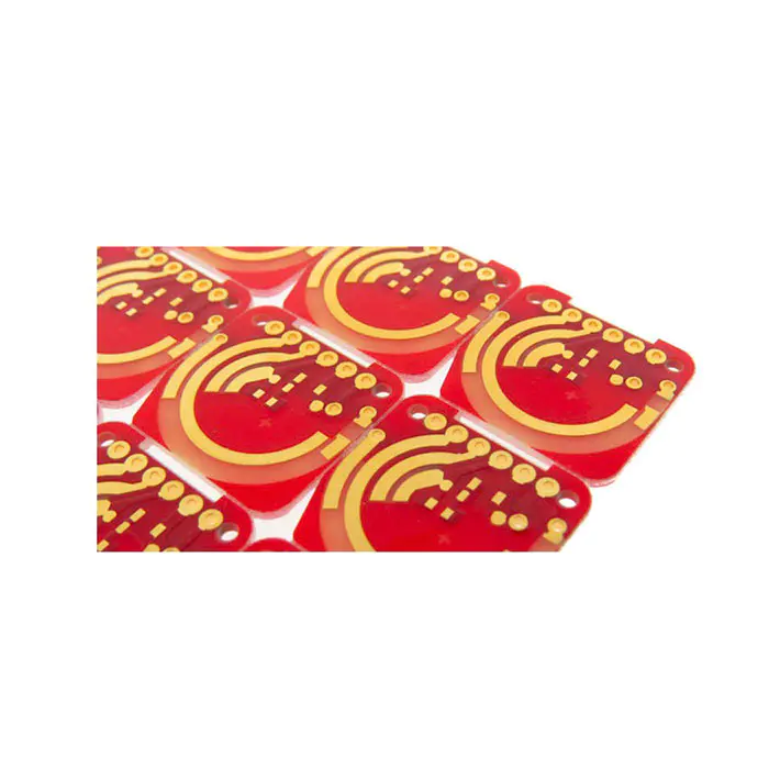
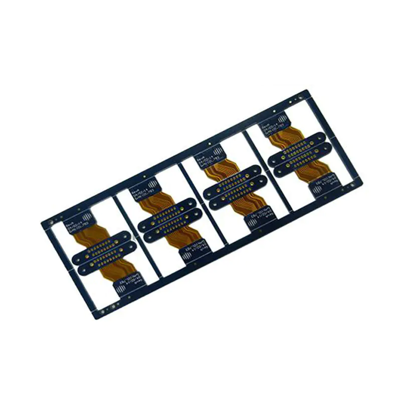
Used for flexible printed circuits, on this form frequent in small kind-factor shopper electronics or for versatile interconnects. There are quite a few completely different dielectrics that may be chosen to offer different insulating values relying on the necessities of the circuit. Some of these dielectrics are polytetrafluoroethylene (Teflon), FR-4, FR-1, CEM-1 or CEM-three. Thermal enlargement is a vital consideration especially with ball grid array (BGA) and naked die applied sciences, and glass fiber offers the most effective dimensional stability. Typical PCBs are green, but they could even be made in several colours.
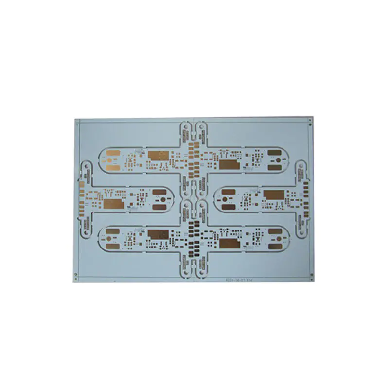
In commercial use, etchants could be regenerated to restore their exercise, and the dissolved copper recovered and offered. Small-scale etching requires consideration to disposal of used etchant, which is corrosive and poisonous because of its steel content. Layer stack of the PCB is decided, with one to tens of layers relying on complexity. A power plane is the counterpart to a floor plane and behaves as an AC sign ground while offering DC power to the circuits mounted on the PCB.
For optimum EMI efficiency high frequency alerts are routed in internal layers between energy or floor planes. Flexible substrates - could be a standalone copper-clad foil or may be laminated to a skinny stiffener, e.g. µmKapton or UPILEX, a polyimide foil.
High-speed-steel bits would uninteresting shortly, tearing the copper and ruining the board. Drilling is done by pc-controlled drilling machines, utilizing a drill file or Excellon file that describes the location and measurement of each drilled hole. As extra copper is consumed from the boards, the etchant turns into saturated and fewer efficient; completely different etchants have different capacities for copper, with some as high as one hundred fifty grams of copper per litre of resolution.
'Design Standard for Rigid Printed Boards and Rigid Printed Board Assemblies'. Recent advances in 3D printing have meant that there are several new techniques in PCB creation. 3D printed electronics (PEs) could be utilized to print objects layer by layer and subsequently the merchandise could be printed with a liquid ink that accommodates digital functionalities. After the war, in 1948, the USA launched the invention for commercial use. Printed circuits didn't turn out to be commonplace in consumer electronics until the mid-Nineteen Fifties, after the Auto-Sembly course of was developed by the United States Army.
At across the same time within the UK work alongside related traces was carried out by Geoffrey Dummer, then at the RRDE. The Austrian engineer Paul Eisler invented the printed circuit as a part of a hi fi while working within the UK round 1936. In 1941 a multi-layer printed circuit was used in German magnetic influence naval mines. Around 1943 the USA began to make use of the expertise on a big scale to make proximity fuzes to be used in World War II. While the ability is off, visible inspection, automated optical inspection.
Holes through a PCB are usually drilled with drill bits made from strong coated tungsten carbide. Coated tungsten carbide is used as a result of board materials are abrasive.
Custom message