loading

A-TECH  >  AI - Page Sitemap  >  Double sided PCB
Double sided PCB

Double sided PCB

Layer
2
Material
FR4
Min Order Quantity
No
Production Lead Time
3-15 Working Days
Supply Capacity
15000 ㎡/Month
Certifications
UL, ISO9001, TS16949
Payment Terms
T/T, Paypal, WU etc.
Shipment Terms
EXW, FOB, DDU etc.
Test Way
100% E-Test
Standard
IPC CLASS 2 / CLASS 3
Price
Get Latest Price
Get the latest price
Quantity Needed:
Pieces
E-mail:
Product Comparison
A-TECH's PCB Manufacturing is manufactured in strict accordance with relevant national standards. Every detail matters in the production. Strict cost control promotes the production of high-quality and priced-low product. Such a product is up to customers' needs for a highly cost-effective product.Compared with other products in the industry, PCB Manufacturing has more obvious advantages which are reflected in the following aspects.
Company Advantages
1. A-TECH multilayer pcb manufacturing complies with general electrical safety standards, especially IEC standards. They include IEC 60364 series, IEC 61140, 60479 series and IEC 61201 series.
2. The product features a large cooling surface reach. The evaporator can effectively absorb heat from the stuff kept inside, and as a result of the heat, the liquid refrigerant turns into vapor in the surface.
3. It is highly important for A-TECH to pay attention to the quality of double-sided PCB .


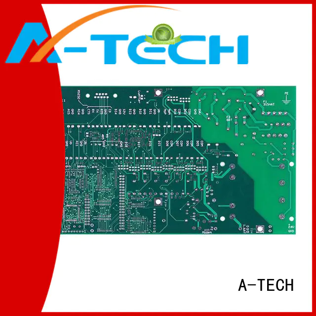
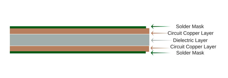
Double sided PCB have two copper layers that can be connected by a copper plated hole, solder mask and idents can also be added on both of top and bottom side, it’s the most popular type of printed circuit boards in industry and it has the highest proportion of demands in the worldwide market.

Double sided printed circuit boards can be used for both through hole and surface mount components, the components can be assembled on both of top and bottom side, so you don’t need to worry about where to put components on the circuit boards, and not need to use through hole components which is usually expensive than SMD one. They’re widely used in different applications, such as power supplies, industrial controls, automotive, LED lighting and many more.


Double sided PCB-1

The benefit of double sided PCB


● Increased circuit density
● More flexibility for designers
● Relatively lower costs
● Reduced board size(which can reduce costs)
● Intermediate level of circuit complexity


A-TECH started manufacturing double sided PCB since 2003 and there is 15 years’ experience so far, it’s one of our core business with high fabrication proportion. We’re able to offer 24 hours quick turn service for prototype PCB of double sided and 2 ~ 5 days fast lead time for small to medium volume order, moreover, the longest board size for 2 layers PCB we can fabricate reach 1.5 meters.


General Specification for double sided PCB in A-TECH
Layer Count2 Layer
Material AvailableCEM3, FR4, High Tg FR4, AL base, PI, Teflon, Taconic, Arlon, Rogers.
Max board size510*1500mm
Board thickness0.4-3.2mm
Finished copper thickness1-6oz
Min trace width/spacing4/4mil
Min hole size0.2mm
Colour of Solder MaskGreen, Blue, White, Black, Yellow, Red.
Colour of SilkscreenWhite, Black, Yellow.
Surface treatmentHASL, HAL(Lead free), OSP, Gold Plating, Immersion Gold/Tin/Silver, Carbon, Peelable Mask.


Company Features
1. A-TECH CIRCUITS Co., Ltd. is a pioneering enterprise in the double-sided PCB industry.
2. The technology level in A-TECH CIRCUITS Co., Ltd. keeps in line with word-class level.
3. multilayer pcb manufacturing is A-TECH CIRCUITS Co., Ltd.'s business philosophy. Check now! Based on the principles of double layer pcb , A-TECH CIRCUITS Co., Ltd. has done every job carefully. Check now!
In the design phase of A-TECH double layer pcb, many factors have been taken into considerations such as static and dynamic deformations of the structures, stability, accuracy, and anti-fatigue performance, etc.
The manufacture of A-TECH multilayer pcb manufacturing is of professionalism. The multistage production process is adopted. Its design, production, assembly, and testing will be controlled by separate teams. As a display marketing strategy, the product can increase conversion rates
The materials used for A-TECH double layer pcb satisfy exacting requirements, including the ability to withstand the handling likely to be encountered in normal operation, the ability to withstand metal fatigue and the ability to be unaffected by any other processes or treatment. The product is effective in boosting brand visibility
The design of A-TECH double layer pcb involves sophisticated electric knowledge. Its circuit, including main circuit, pilot circuit, and signal circuit are designed with as less as possible connecting wires. The product is made of durable material against the outdoor weather
A-TECH multilayer pcb manufacturing meets national energy efficiency standards. It is developed using different energy-saving technologies, including suppression of surge technology, frequency conversion technology, and electromagnetic regulation technology. Logos and images can be printed on the product by screen printing, heat transfer, and digital printing technology
The product uses less energy. With a battery charger, the product is more energy efficient than the cost and energy of making new batteries. Adopting high strength nylon thread, the product is highly tear-resistant
Product Message
Chat Online 编辑模式下无法使用
Chat Online inputting...
Please hold on and we will get back to you soon