Latest products
Circuit board processing should pay special attention to what point?
by:A-TECH
2020-05-15
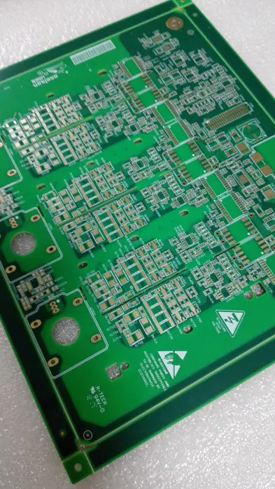
General circuit board processing is based on circuit principle based on the graph design, so as to achieve the required functions.
The layout of the printed circuit board needs to consider each part connection, more attention should be paid to optimize components.
Optimization line and hole, electromagnetic protection, heat dissipation and other factors.
Generally a good circuit design, is to save the production cost, good performance, thermal performance.
So we should pay special attention to the following points: one, using filling piece drawing pad with filling solder when designing circuit can through the DRC check, but the processing is no good, so kind of bonding pad can not directly generate resistance welding data, in resistance welding flux, the filling area will be covered by the ink curing, lead to a difficult components welding assembly.
Second, place 1, the character of the characters, SMT solder, on-off testing and components to printed circuit board welding inconvenience.
2, the character design is too small, resulting in the difficulty of the silk screen printing, overlapping characters of too much, it is difficult to distinguish.
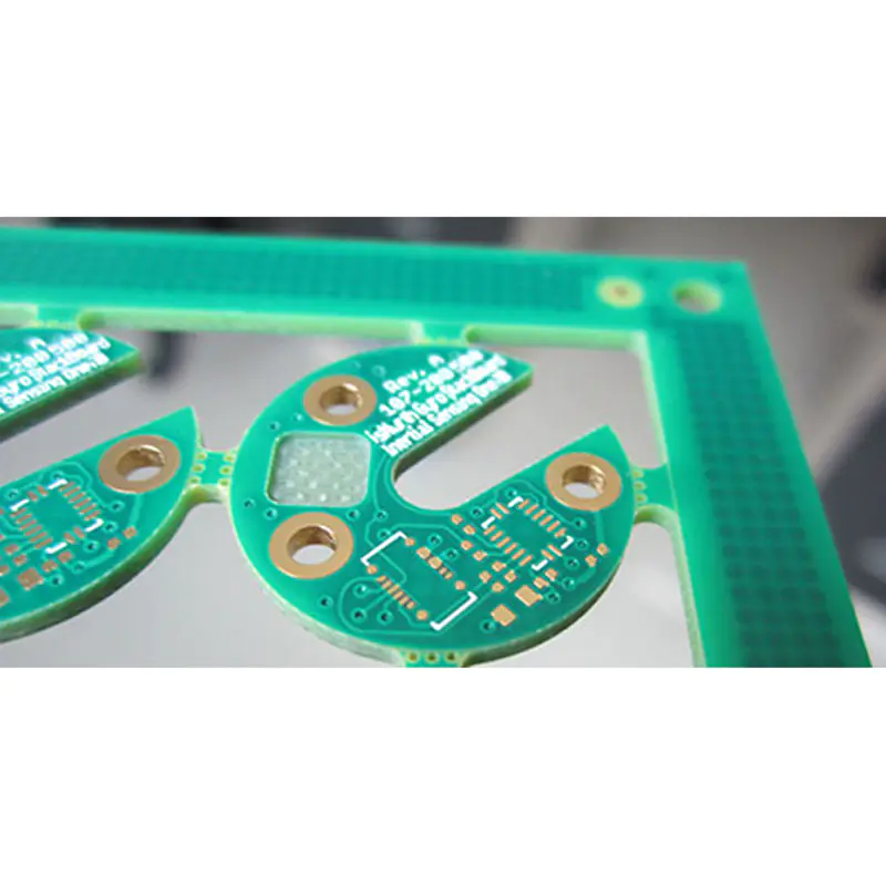
Three, large area of copper foil too close to the distance from the casing outside the large area of copper foil from outside the box should be at least 0.
More than 2 mm spacing, because when milling shape such as milling on the copper foil cause copper foil case become warped and flux loss caused by the resistance problem.
Four, large area of the grid spacing is too small of the edge of the area between grid lines and line is too small (
Less than zero.
3毫米)
, in the process of PCB manufacturing, figure after turning process on the shadow prone to a lot of film adhesion on the board, bolt.
Five, solder overlap (
Drilling overlap)
1, the bonding pad (
In addition to the surface welding this)
Overlapped overlap, meaning that hole, drilling in the drilling process in one place many times lead to broken bit, leading to loss of hole.
2, two holes in a multilayer overlap, such as for the isolation of a hole plate, a hole for the connection plate (
Spend bonding pad)
So that after the paint film performance for isolation plates, scrap.
Six, the abuse of PCB graphics layer 1, in some attachment did some useless graphics layer, was four layer board is designed five floors above the line, make the misunderstanding.
2, when the design graph save trouble, with Protel software as an example for some lines in every layer Board layer to paint, and with Board layer to delimit dimensioning lines, which, when light painting data layer Board, because not to miss the attachment and open circuit, or because of the selection Board layer labeling lines and short circuit, so keep the graphics layer when the design is complete and clear.
3, in violation of the conventional design, such as component design on the Bottom floor and welding surface design on the Top, causing inconvenience.
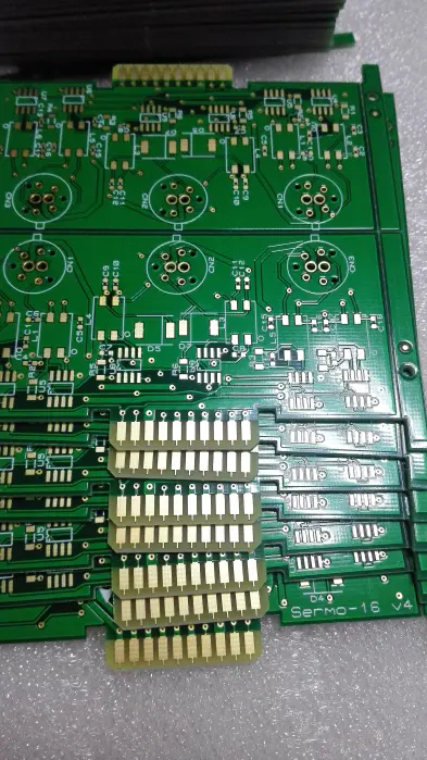
Seven, surface-mount device bonding pad too short this is for on-off testing, for SMT components is too close, the spacing between the two feet is fairly small, welding plate is also quite thin, installation testing needle, must be up and down,
Or so)
Staggered position, such as welding plate design is too short, although does not affect the device installation, but can make the test needle wrong doesn't open.
Custom message