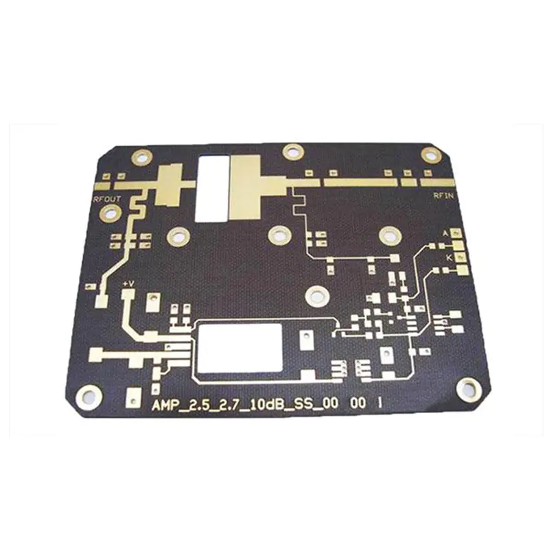
Latest products
Circuit board processing methods what are resistance to electromagnetic interference
by:A-TECH
2020-05-12
1, signal layer of the main circuit board processing information interaction is with three signal layers, these signals with wiring and welding, placed in the circuit board processing components and signal lines, and gives some normal information service functions, circuit board processing.
Under the use of the information layer circuit board processing shows good capability of information interaction, using this circuit board processing can achieve better ability of electronic control.
2, internal power supply circuit board processing of signal layer and inner into additive through aperture connected to each other to achieve a better electronic operation ability, and the internal power supply layer is unique to the circuit board processing of parts, under the use of the internal power supply layer, to be able to become better connections between the classes.
3, mechanical layer of circuit board processing machinery city a way, related process and the preparation method of indicative information accessories, in the use of a multilayer able to draw up the PCB of the frame and place the better processing technology, to achieve page simple planning, also make the process of connecting the mechanical layer more clear and lively.
We analyse the circuit board processing methods what are resistance to electromagnetic interference.
1, control the interference source circuit board processing in the actual application of want better anti-interference, you can use low value of inductance of accessories to reduce electric pole and signal layer signal problems, in addition to signal lines placed in the same power PCB layer and layer as far as possible close to the ground plane, only in this way can will be possible as far as possible avoid electromagnetic interference factors, make the circuit board processing presents more good anti-interference effect.
2, pay attention to the layout of the parts now have experience in the actual design of the circuit board processing manufacturer, to block processing of parts, process layout of the parts separate weak electrical signals, the digital signal circuit and simulator and separately in each circuit of the filtering network connection to the nearest, which can improve the anti-interference ability of the circuit board processing.
3, the optimization of the circuit board processing in the use of unreasonable layout wiring will cause the interaction between the signal interference, so the power cord when circuit board processing of wiring widened as possible to reduce the loop resistance, signal lines shorten the reduced number of holes, should as far as possible to expand the corner Angle when wiring, so can make wiring conforms to the requirement of building use.
Custom message