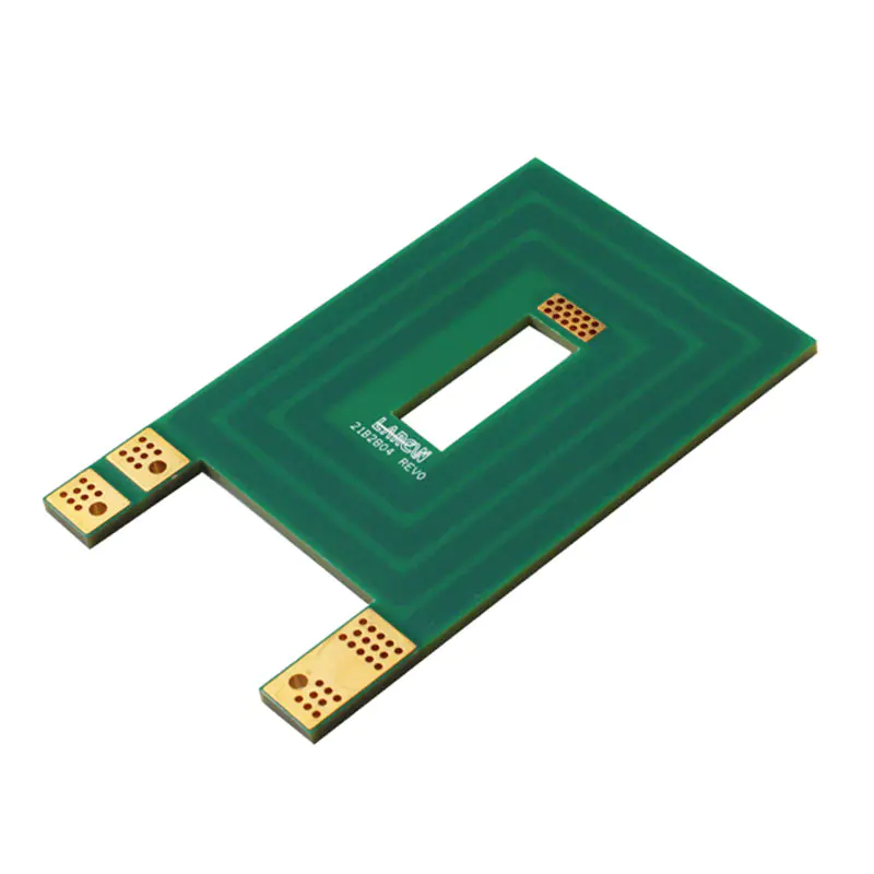
Circuit board processing and wiring should be on the correct operation rules and constraint conditions
by:A-TECH
2020-05-17
Circuit board processing design is a key and time consuming task, any questions are need to check the whole design engineer one by one network element.
To say the circuit board processing degree of careful design requirements as chip design.
In both manufacturing assembly process and in actual use, the PCB must have reliable performance, it is very important.
In addition to the relevant cost, the defects in the process of assembling PCB into product, is the likely failure may occur in the process of actual use, result in a claim against you.
In that sense, therefore, can never to say that the cost of a high quality PCB is negligible.
In all market segments, especially in the production of key application in the field of product in the market, the consequences of such failure.
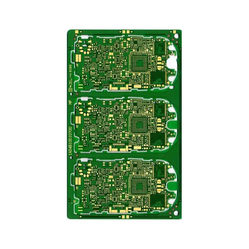
Circuit board processing mission to smoothly finished wiring, wiring things need to be accurate operation rules and constraint conditions.
To categorize all special request signal, each signal class should have priority, the higher the priority, the rules are more strict.
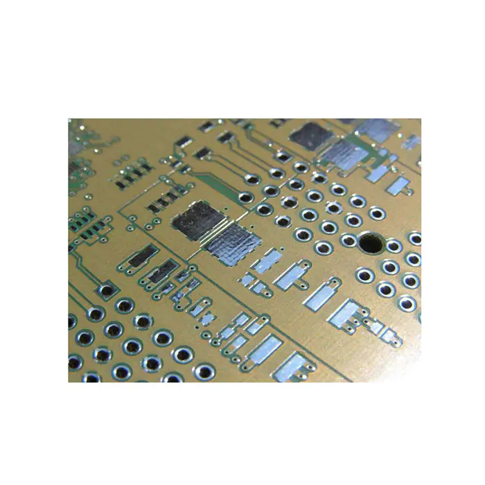
Hit a printing line width, via the rules large quantity, parallelism, the mutual influence between line and constraint layer, these rules has a great influence to the function of wiring things.
Circuit board processing scale and wiring layer needs to be decided at the early stage of the plan.
The number of wiring layer and layer (
堆栈,
)
Method will directly affect the printing line wiring and impedance.
Intrusive helps to conclude that cascading method of plate and printing line width, hope to end the program.
Now a multilayer capital between different is very small, when start plans better choose more copper circuit layer and apply evenly distributed.
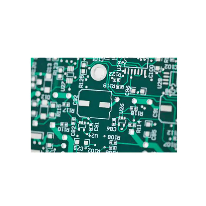
PCB layout rules: 1, under normal circumstances, all components shall be set on the boards of the same, only the top-level element too close, to get some highly limited and calorific value small devices, such as SMD resistor, SMD capacitors, SMD IC in the lower level.
2, on the premise of guarantee the electrical performance, elements should be placed on the grid and parallel or vertical arrangement, in order to tidy, beautiful, in the general case does not allow components overlap;
Element is arranged to compact, element in the page layout should be uniform distribution, the density is consistent.
Three different components on printed circuit boards, small spacing between neighboring solder graphics should be more than 1 mm.
4, away from the circuit board edge is generally not less than 2 mm.
Circuit board of the shape of rectangular, length-width ratio of 3:2 or 4:3.
Circuit board face 'is greater than 200 mm by 150 mm, consideration should be given circuit board can withstand mechanical strength.
Custom message