Circuit board processing and processing process preheating which steps
by:A-TECH
2020-05-20
The circuit board from single to double side, multi-layer and flexible, and their development trend remained.
Due to the constantly to develop in the direction of high precision, high density and high reliability, shrinking volume, reduce costs, improve performance, making PCB circuit boards in the future development of the electronic equipment engineering, still maintained a strong vitality.
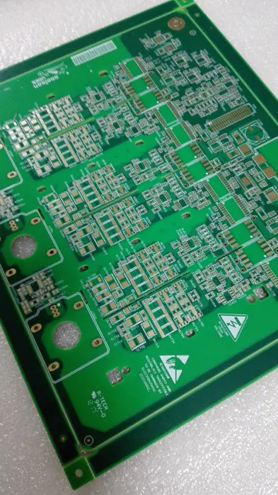
Circuit board processing and assembling electronic design personnel must have a skill.
Is in order to avoid high temperature when welding circuit board suction and critical plate, tin, blow hole, solder joint cavity, and problems for the purpose of, have long-term storage of the board should first baking, to remove water may be inhaled.
After drying cooling board in 2 - as quickly as possible
Within 3 days after welding, to avoid water absorption grow again.
The following is the circuit board processing and assembly for preheating.
1, the board and the temperature of the parts, reduce the moment into the dangers of thermal stress caused by high temperature, and can improve the ability of liquid tin melting into the hole.
2, get rid of the volatile component of flux decrease subsequent conveyor rapid production welding splash in the tin, tin or PTH hole to fill the void, or solder paste filling point of gas holes, etc.
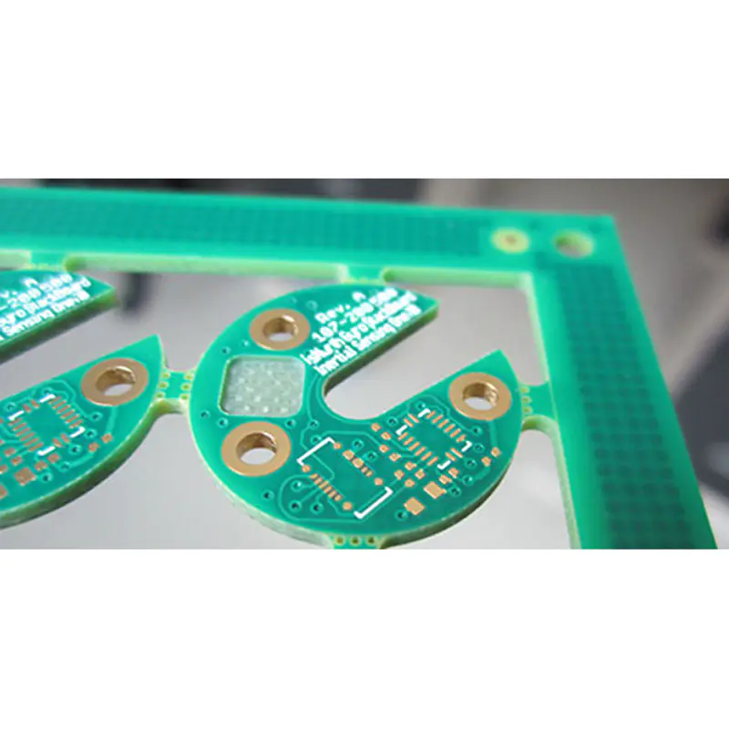
Need to go through a lot of PCB process, in which the preliminary drying is one of the more important, and the coating process are generally the same room.
Preliminary drying refers to make through heating drying liquid photo imageable etching resist agent reached at the membrane surface is dry, with convenient contact double-exposed development create graphics.
And other technology to the quality of the circuit board processing.
Increase the activity of flux and ability, to make easier to remove oxide with dirt on the surface of the weld, increase its solder, this point is especially important for corner point such as the 'protected area'.
Domestic auto detection system for printed circuit board research began in the 90 s brought about, still just getting started.
At present, scientific research institutes engaged in research on this aspect is less, but also because of the influence of various factors, automatic optical inspection system for printed circuit board defects research also stays at a relatively early levels.
Because of foreign PCB automatic testing system is too expensive, and did not develop domestic PCB automatic testing equipment on real significance, so most of the domestic electronics assembly processing manufacturers still use manual with a magnifying glass or projector to check the way to test.
Because human check the intensity of labor is big, easy to produce fatigue, eye leak inspection rate is very high.
And with the development of electronic products towards miniaturization, digitalization, printed circuit board is toward the development of high density, high precision, adopt the method of artificial test, basic cannot be achieved.
Custom message