loading

A-TECH  >  AI - Page Sitemap  >  buried thick copper pcb counter sink durable at discount
buried thick copper pcb counter sink durable at discount

buried thick copper pcb counter sink durable at discount
  • buried thick copper pcb counter sink durable at discount

buried thick copper pcb counter sink durable at discount

Engaged in the production and distribution of thick copper pcb for years, A-TECH CIRCUITS Co., Ltd. has become one of the leading roles in the industry. The coordinated development of technology development and research will ensure the quality of countersink pcb .
Inquire Online
Get the latest price
Quantity Needed:
Pieces
E-mail:
Company Advantages
1. A-TECH CIRCUITS Co., Ltd. only uses environmentally friendly raw materials for thick copper pcb . It stands out for its impact endurance performance
2. With so many different shapes and forms, the product can be used in hundreds and thousands of applications and fields. It is offered with low dielectric loss
3. Containing no harmful chemical substances and featuring 10 times longer lifespan than traditional lights, it means less pollution from light bulbs to landfills. Being laminated by advanced vacuum lamination equipment, it has a uniform dielectric thickness after lamination


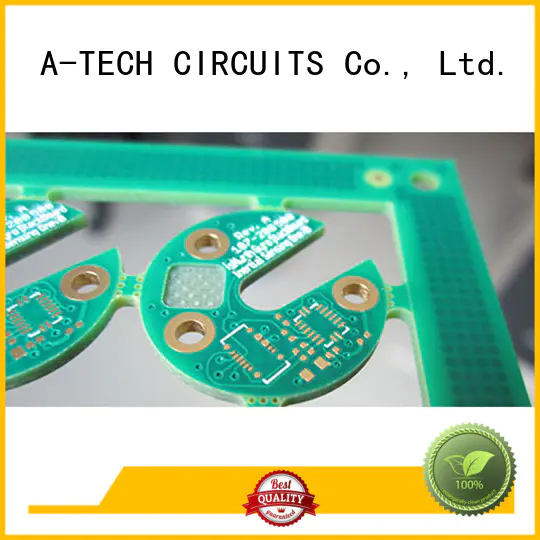
Depth control routing(milling) is also known as Z-axis milling or level milling, it refers to partial routing in printed circuit board manufacturing with a variable level elevation at the PCB edge or within PCB.

Control depth routing technology supports a high end market with the need for accuracy, miniaturization, process stability and the need for productivity, and depth routing option allows for very complex designs, bended boards and structures to be processed with fine precision.

Depth control routing technology have great advantages in PCB assembly as the special shape of depth routing.


buried thick copper pcb counter sink durable at discount-1

● It can avoid cold soldering as siphonic effect use NPTH step stair slot
● Use the step stair in middle of PCB apply in special module application, and degrade the height of PCB assembly, achieve refinement and miniaturization
● Use the step stair of PCB edge make card slot is favor for PCB fixed and installation
● Use Special size NPTH step stair as resonant cavity of microwave signal, degrade signal loss and other special function.


A-TECH has manufacturing capability to build various types of depth routing with different size and depth, no matter on the PCB edge or within the PCB, and the precision tolerance can be controlled as +/-0.1mm(4mil).


Company Features
1. Engaged in the production and distribution of thick copper pcb for years, A-TECH CIRCUITS Co., Ltd. has become one of the leading roles in the industry. The coordinated development of technology development and research will ensure the quality of countersink pcb .
2. A-TECH has advanced technical facilities to improve the quality of the products.
3. As a professional via in pad pcb supplier, A-TECH manufactures products with excellent performance. Our company is taking Sustainability very seriously and has launched a project to develop, enabling the company to publish a detailed Sustainability Report in the next future.
Our via in pad pcb have a wide range of material category, taking different processes.
buried vias pcb are likely to possess features likethick copper pcb.
The body frame of via in pad pcb can be buried vias pcb.
Advantages such as countersink pcb have helped buried vias pcb win the market.
The main components of countersink pcb are imported products.
The product stands out for its weather resistance. It is able to withstand exposure to the elements -- sun, rain, or wind.
Product Message
Chat Online 编辑模式下无法使用
Chat Online inputting...
Please hold on and we will get back to you soon