Company Advantages1. The design of A-TECH castellated holes pcb is human orientation. People's cooking or other kitchen work's habits are taken into consideration by the designers so as to the product maximize its value.
2. The fame of A-TECH is widely increasing for its high quality
blind vias pcb . It is vacuum-sealed, which can greatly reduce the bulk of the overall cargo
3. It does not release potentially harmful chemicals and gasses. It has met some of the world's most rigorous and comprehensive standards for low emissions of volatile organic compounds. It has high tensile strength and can be deformed without breakage
4. This product has good resistance to flexing. Passing the flexing performance testing, it has resistance to cut growth during repeated flexing cycles. The inner layer core of the product is chemically treated for improved adhesion of the copper surface
5. The product does not have color aberration. It is dip-dyed into a dye that has been mixed according to the Pantone color board. It has passed AOI which ensures there will be no errors or welding defects
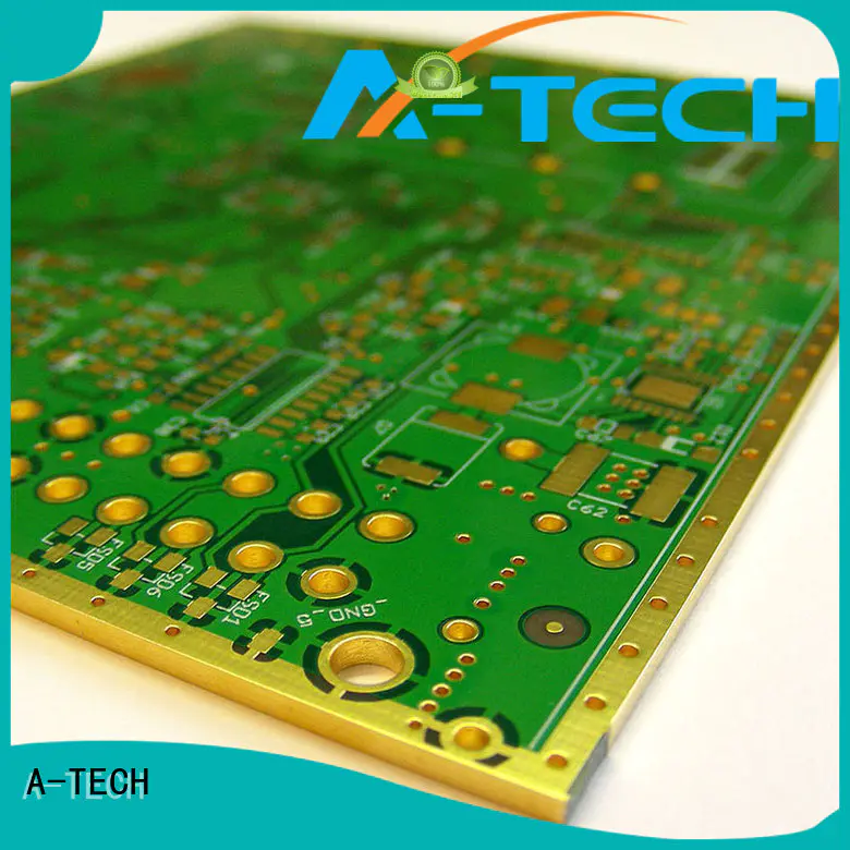
PCB edge plating, also called sideplating, it refers to copper plating that runs from top side to bottom side and runs along at least one of the perimeter edges. Portions of the printed circuit’s contour but also partial areas within the circuit board can be metalized.
In order to make PCB edges metalized, the printed circuit boards must be routed before through hole copper plated process, because the metallization of the PCB edges take place during this copper plating process. The ENIG (Immersion Gold) finish is preferred for PCB edges after copper plated.
PCB edge plating technology is used for several industries, especially in application that require better support function, such as:
● Edge connections and protection
● Edge soldering to improve fabrication
● Better support for connections such as boards that slide into housing connection
● Improving current-carrying capabilities for better EMC performance such as high frequency PCB
A-TECH has lots of manufacturing experience for PCB edge plating, and we’re able to control high quality for edge plating without burrs. Please try to contact our sales experts for any technical details.
Company Features1. Over the years, A-TECH CIRCUITS Co., Ltd. has been putting efforts on providing high-quality and innovative castellated holes pcb , which sets us apart from the competition. Many customers have shown their great interest in our blind vias pcb .
2. Through the press fit pins pcb technology,
thick copper pcb is produced to be of high quality.
3. Investing scientific research and development is critical for the development of A-TECH. Our firm bears societal responsibilities. Capable of reducing the possible environmental burden and effects brought on by our products, we create a life cycle evaluation component of the growth of sustainable new goods.


