Company Advantages1. A-TECH buried vias pcb is fabricated using quality raw materials and advanced production technology.
2. This product has excellent impact resistance. Its high compressibility and rebound resilience allow it to work under high-pressure mechanical movement.
3. The product performs well in heat resistance. The materials used in it have a high coefficient of heat conductivity and a relatively low coefficient of linear expansion which make it not prone to fracture under high temperature.
4. The high commercial value gives the product a wide market application.
5. The product is actually a lot more durable than standard light bulbs. It can withstand a lot of damage before it breaks.
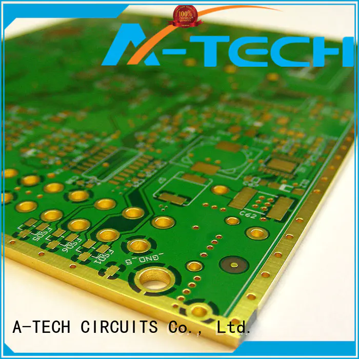
PCB edge plating, also called sideplating, it refers to copper plating that runs from top side to bottom side and runs along at least one of the perimeter edges. Portions of the printed circuit’s contour but also partial areas within the circuit board can be metalized.
In order to make PCB edges metalized, the printed circuit boards must be routed before through hole copper plated process, because the metallization of the PCB edges take place during this copper plating process. The ENIG (Immersion Gold) finish is preferred for PCB edges after copper plated.
PCB edge plating technology is used for several industries, especially in application that require better support function, such as:
● Edge connections and protection
● Edge soldering to improve fabrication
● Better support for connections such as boards that slide into housing connection
● Improving current-carrying capabilities for better EMC performance such as high frequency PCB
A-TECH has lots of manufacturing experience for PCB edge plating, and we’re able to control high quality for edge plating without burrs. Please try to contact our sales experts for any technical details.
Company Features1. Engaged in
via in pad pcb production for many years, A-TECH CIRCUITS Co., Ltd. has become a leading company.
2. With great service and excellent product quality, not only have we won the overseas markets, but we have also been rewarded praises from domestic and foreign customers.
3. We recognize our responsibility to reduce our contribution to global climate change. We work to conserve energy, invest in renewable sources of energy, and reduce our greenhouse gas (GHG) emissions. Customers are the key factor in our success. We try our best to gain deep knowledge of the market trends of the products and closely cooperate with other companies to create distinctive and targeted products. Regarding our efforts to promote sustainable development, we are not only responsible for clients, but also responsible for society, the country, and the future. We will make our business activities and production more sustainable.


