Answers to common questions during PCB design
by:A-TECH
2021-04-07
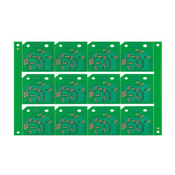
We will encounter many kinds of problems in PCB learning, and these problems also cover all aspects. What should we do when we encounter these problems? Next, I will introduce some common problems for you. One. What is the meaning of part packaging and what is the difference between it and parts? (1) The package of parts refers to the appearance and location of solder joints indicated when the actual parts are soldered to the circuit board. (2) Part packaging is only the appearance of the part and the location of the solder joints. The pure part packaging is only the concept of space, so different parts can share the same part packaging; on the other hand, the same kind of parts can also have different packaging, such as RES2 stands for resistance, and its packaging forms are AXAIL0.4, AXAIL0.3, AXAIL0.6, etc., so when using welding parts, you must know not only the name of the part but also the package of the part. (3) The package of parts can be specified when designing the circuit diagram, or when the netlist is introduced. When designing the circuit diagram, you can specify it in the Footprint setting item in the part properties dialog box, or you can specify the part package when importing the netlist. Two basic knowledge of reflected signals in PCB design The main reasons for reflected signals are: excessively long traces; unmatched termination of transmission lines, excessive capacitance or inductance, and impedance mismatch. If terminal matching is not considered sufficiently, EMI will increase significantly, which will not only affect the results of its own design, but will also cause the entire system to fail. Three delays and timing errors Signal delay causes: drive overload, wiring is too long. Signal delay and timing errors are manifested as: the signal does not jump for a period of time when the signal changes between a high logic level and a low threshold. Excessive signal delay may cause timing errors and device function disorder. Four times crossing the logic level threshold error reflected signal causes: too long traces, unterminated transmission lines, excessive capacitance or inductance, and impedance mismatch. The signal may cross the logic level threshold many times during the transition process and cause this type of error. The error of crossing the logic level threshold multiple times is a special form of signal oscillation, that is, the signal oscillation occurs near the logic level threshold, and crossing the logic level threshold multiple times will cause the logic function disorder. Five overshoot and undershoot Overshoot and undershoot come from two reasons: the trace is too long or the signal changes too fast. Although most component receiving ends are protected by input protection diodes, sometimes these overshoot levels will far exceed the component power supply voltage range and damage components. Six crosstalk crosstalk is manifested in that when a signal passes through a signal line, related signals will be induced on the adjacent signal line on the PCB, which is called crosstalk. The closer the signal line is to the ground line, the greater the line spacing, and the smaller the crosstalk signal generated. Asynchronous signals and clock signals are more prone to crosstalk. Therefore, the crosstalk method is to remove the crosstalk signal or shield the severely interfered signal. Seven Electromagnetic Radiation EMI is electromagnetic interference. The problems caused include excessive electromagnetic radiation and susceptibility to electromagnetic radiation. EMI is manifested in that when the digital system is powered on, it will radiate electromagnetic waves to the surrounding environment, thereby interfering with the normal operation of electronic equipment in the surrounding environment. The main reason for it is that the operating frequency of the circuit is too high and the layout is unreasonable. There are software tools for EMI simulation, but EMI simulators are very expensive, and it is difficult to set simulation parameters and boundary conditions, which will directly affect the accuracy and practicability of the simulation results. The most common approach is to apply the various design rules for controlling EMI in every aspect of the design, so as to realize the rule-driven and control in every aspect of the design. The above-mentioned basic questions are commonly used in daily life, and I hope it can be helpful to beginners.
Custom message