via in pad pcb-multilayer pcb manufacturing process We ensure that customers get the most out of via in pad pcb-multilayer pcb manufacturing process as well as other products ordered from A-TECH PCB and make ourselves available for all related questions, comments, and concerns.
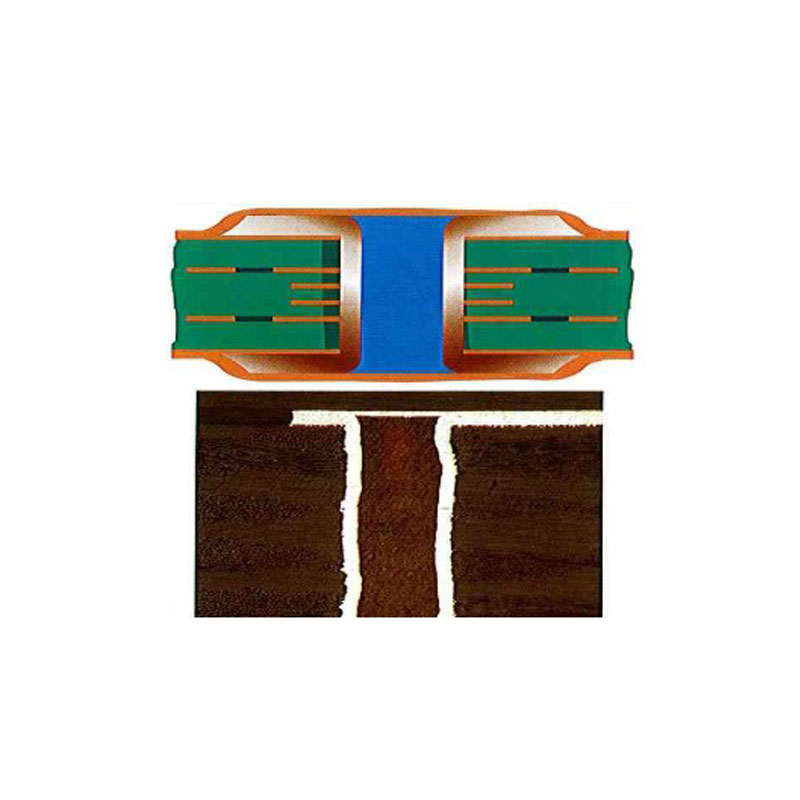
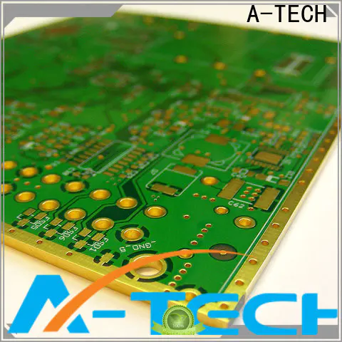
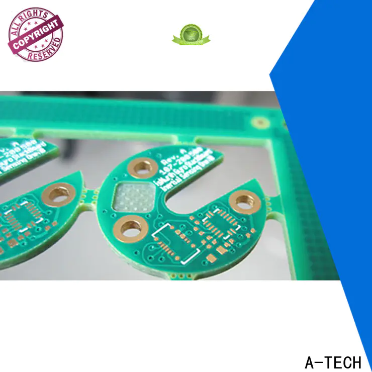
A-TECH via in pad pcb-multilayer pcb manufacturing process via in pad pcb-multilayer pcb manufacturing process is a sought-after product in A-TECH CIRCUITS Co., Ltd.. It is designed to impress people all over the world. Its look combines the complex design theory and hands-on knowledge of our designers. With a team of highly qualified experts and state-of-the-art equipment, we promise the product has the advantages of stability, reliability, and durability. Our QC team is well-equipped to perform the indispensable tests and ensure the defective rate is lower than the average rate in the international market.metal core pcb,pcb prototype board,double-sided pcb.