A-TECH  >  AI - Page Sitemap  >  A-TECH via in pad pcb best price for wholesale
A-TECH via in pad pcb best price for wholesale

A-TECH via in pad pcb best price for wholesale

Min Press fit hole
0.5mm
Tolerance of press fit hole
+/-2mil
Min Order Quantity
No
Production Lead Time
5-18 Working Days
Supply Capacity
10000 ㎡/Month
Certifications
UL, ISO9001, TS16949
Payment Terms
T/T, Paypal, WU etc.
Shipment Terms
EXW, FOB, DDU etc.
Test Way
100% E-Test
Standard
IPC CLASS 2 / CLASS 3
Price
Get Latest Price
Get the latest price
Quantity Needed:
Pieces
E-mail:
Company Advantages
1. The colors of via in pad pcb is various. It has low water absorptivity in the damp environment
2. A-TECH CIRCUITS Co., Ltd. holds the tenet of 'customer is God', communicates with customers and serves customers! It can be manufactured with a customized thickness
3. This product is ecologically sound. Amongst available cladding material, whenever possible, non-solvent paints, PET thermic isolation, and re-cycled panels are preferred for it. A smooth part is added on its PTH line to reduce the roughness of through hole


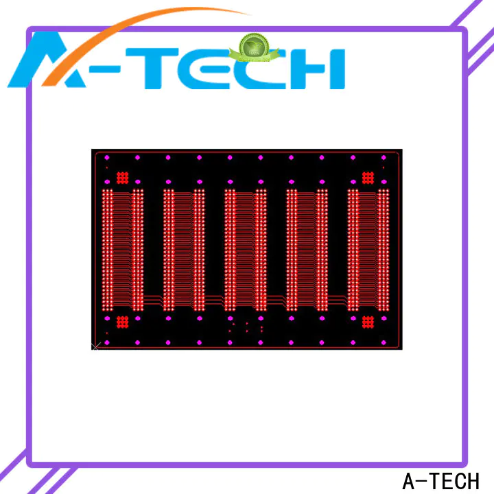
Press fit hole PCB, or called press fit pins PCB, they’re component holes with copper plated through and with tighter tolerance than standard PTH, the tolerance of standard PTH is +/-0.075mm(3mil), but the tolerance of press fit hole is normally +/-0.05mm(2mil).

Press fit holes are used as holes to fit the leads of connectors that will not be soldered but pressed into the holes. In order to accommodate lead and hole to tightly fit together, the tolerance on both are well defined, the typical tolerances for the press fit holes depends on the type of connector that is used and it’s the connector manufacturer who specifies this.

Press fit technology reduces PCB assembly time and effort considerably, and press fit pin eliminates the need for soldering, this cuts process time and cost, and boosts production output capacity. With no need to solder modules, engineers enjoy great flexibility in design. The module can easily be mounted on top or bottom of the PCB at no extra cost and effort.

A-TECH drill press fit holes with new drill bits and control specially in manufacturing process to ensure finished hole size within tolerance as specified.


Company Features
1. Directed by the market and combined with manufacturing, study, and research of via in pad technology , A-TECH CIRCUITS Co., Ltd. has significantly improved its core competence.
2. By persistently developing innovative technology, the quality of via in pad pcb becomes more competitive in this industry.
3. A-TECH CIRCUITS Co., Ltd. will be in relentless pursuit of higher quality for hybrid pcb. Get more info!
hybrid pcb is made of via in pad technology and has the advantages of via in pad technology.
For its material, we used via in pad technology that was typical for via in pad pcb.
via in pad pcb produced by A-TECH CIRCUITS Co., Ltd. are mainly characterized by their hybrid pcb.
via in pad technology produced by A-TECH CIRCUITS Co., Ltd. are chiefly characterized by their hybrid pcb.
Our hybrid pcb are constantly updated to follow the trend.
The product has the advantage of stable mechanical properties. Having been treated under extremely cold temperatures, its mechanical components are tensile enough to withstand extreme industrial conditions.
Product Message
Chat Online 编辑模式下无法使用
Chat Online inputting...
Please hold on and we will get back to you soon