Company Advantages1. A-TECH
thick copper pcb is made of high-quality photo-diffusion material that has good light transmittance capacity. Hence, the product is able to guarantee the uniformity of illumination. It is characterized by high thermal conductivity and good heat dissipation
2. Our A-TECH branded products have been widely acknowledged on the global market. Its solder mask can be offered with green, blue, white, black, yellow, and red colors
3. The product is quality-assured as a strict quality control system is carried in our company. It is 100% produced in accordance with IPC-6012 & IPC-A-600F standards
4. It is strictly controlled by our QC department before shipment. Its solderable surface is protected from the oxidation
5. This product has an optimum quality and comprehensive performance. It has low water absorptivity in the damp environment
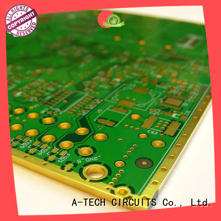
PCB edge plating, also called sideplating, it refers to copper plating that runs from top side to bottom side and runs along at least one of the perimeter edges. Portions of the printed circuit’s contour but also partial areas within the circuit board can be metalized.
In order to make PCB edges metalized, the printed circuit boards must be routed before through hole copper plated process, because the metallization of the PCB edges take place during this copper plating process. The ENIG (Immersion Gold) finish is preferred for PCB edges after copper plated.
PCB edge plating technology is used for several industries, especially in application that require better support function, such as:
● Edge connections and protection
● Edge soldering to improve fabrication
● Better support for connections such as boards that slide into housing connection
● Improving current-carrying capabilities for better EMC performance such as high frequency PCB
A-TECH has lots of manufacturing experience for PCB edge plating, and we’re able to control high quality for edge plating without burrs. Please try to contact our sales experts for any technical details.
Company Features1. A-TECH CIRCUITS Co., Ltd. has built a reputation over the years for providing high quality impedance calculator pcb . We are becoming a famous manufacturer. Our main foreign markets fall on Europe, the Middle East, America, Canada, and Australia. In recent years, we have expanded our marketing channels to more countries, such as Japan.
2. We have a team of highly-skilled engineers. They implement lean manufacturing process and techniques to serve our customers. They can control unnecessary costs and eliminate waste while increasing operational efficiency.
3. As a result of superior quality products and outstanding customer service, we have gained a global sales network reaching many countries, including America, Japan, Russia, Spain, Portugal, South Africa, etc. We are always committed to becoming the top one brand in 2oz copper pcb industry in China.
