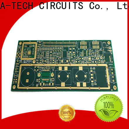
A-TECH  >  AI - Page Sitemap  >  A-TECH quick turn pcb shop double sided
A-TECH quick turn pcb shop double sided

A-TECH quick turn pcb shop double sided

Layer
4
Material
FR4(Tg170)
Min Order Quantity
No
Production Lead Time
1-9 Working Days
Supply Capacity
5000 ㎡/Month
Certifications
UL, ISO9001, TS16949
Payment Terms
T/T, Paypal, WU etc.
Shipment Terms
EXW, FOB, DDU etc.
Test Way
100% E-Test
Standard
IPC CLASS 2 / CLASS 3
Price
Get Latest Price
Get the latest price
Quantity Needed:
Pieces
E-mail:
Company Advantages
1. The labeling of A-TECH single layer pcb is ensured to contain all required information including registered identification number (RN), country of origin, and fabric content/care. It has increased power densities which guarantee its long service life
2. A-TECH CIRCUITS Co., Ltd. has established a fairly complete management system for pcb shop production. It has high tensile strength and can be deformed without breakage
3. The product is not prone to oxidization. Through an electrical process to form a certain layer of an anodic layer on its surface, it is not affected by the air or moisture.


Quick turn PCB prototype manufacturing is one of characteristic service in A-TECH with special sample team to follow the whole production schedule. We fully understand short and accurate lead time is essential in today’s rapidly changing market place. Customers need to know the exact date of the circuit boards delivery so they can prepare the project schedules ahead of time.

We calculate and control each manufacturing process in the unit of hour to ensure the minimum time wasted in production. Currently the fastest lead time we can achieve for prototype PCB is 24 hours delivery for double sided PCB, 48 hours for 4 to 6 layers and 72 hours for 8 or more high multilayer PCB.

Moreover, we're different with most of prototype pcb manufacturers with online orders, whom 100% follow the gerber files you submit online to build, no matter it’s correct or there are some errors on design. Our engineering group offer DFM (design for manufacturing) service before manufacturing, we'll submit engineering questions to confirm and communicate with customers to optimize designs or avoid any potential errors.


The standard and fastest lead time for prototype PCB in A-TECH
LayerFastest Lead TimeStandard Lead Time
224 Hours4 WDs
448 Hours5 WDs
648 Hours6 WDs
872 Hours7 WDs
1096 Hours8 WDs
1296 Hours8 WDs
14120 Hours9 WDs
≥16Up to difficultyUp to difficulty


Company Features
1. With years of experience in single layer pcb R&D and manufacturing, A-TECH CIRCUITS Co., Ltd. is a reputable and professional supplier in the domestic market. A-TECH CIRCUITS Co., Ltd.'s R&D capability has highlighted through pcb shop .
2. With solid technology foundation, A-TECH CIRCUITS Co., Ltd. is up to a high level of domestic technology.
3. A-TECH CIRCUITS Co., Ltd. has greatly enhanced the R&D ability for pcb fabrication assembly production. From improving the quality of support, A-TECH will pay additional attention to the culture institution. Contact!
A range of reliable tests for A-TECH pcb fabrication assembly will be carried out by the QC team. It has passed the anti-aging test, high-temperature resisting test, and shock-proof tests. It can be manufactured with a customized thickness
Testing for A-TECH single layer pcb is performed thoroughly. These tests are performed on its mechanical parts, materials and the entire structure to ensure its mechanical properties. It has passed AOI which ensures there will be no errors or welding defects
All of the materials used in A-TECH pcb fabrication assembly are required to meet relevant demands. The hardware or mechanical components will be tested for mechanical properties and chemical composition. It is 100% produced in accordance with IPC-6012 & IPC-A-600F standards
The design of A-TECH pcb fabrication assembly requires many skills. Except for basic knowledge such as Kinematics and Mechanisms, they also include Technical Drawing and Computer-Aided Engineering (CAE). It is characterized by high thermal conductivity and good heat dissipation
The design of A-TECH single layer pcb is the integration of intelligence and professionalism. The latest cutting-edge technologies such as automation detection and automatic control technologies have been applied to its design. Being laminated by advanced vacuum lamination equipment, it has a uniform dielectric thickness after lamination
[企业简称] organizes production in strict accordance with national standards and product technical requirements. The pcb fabrication assembly manufactured is fine in workmanship, exquisite in shape, excellent in performance and reliable in quality, and enjoys a high reputation in the market.
Product Message
Chat Online 编辑模式下无法使用
Chat Online inputting...
Please hold on and we will get back to you soon