loading

A-TECH  >  AI - Page Sitemap  >  A-TECH ODM high quality pcb edge plating process hot-sale for sale
A-TECH ODM high quality pcb edge plating process hot-sale for sale

A-TECH ODM high quality pcb edge plating process hot-sale for sale

Min Press fit hole
0.5mm
Tolerance of press fit hole
+/-2mil
Min Order Quantity
No
Production Lead Time
5-18 Working Days
Supply Capacity
10000 ㎡/Month
Certifications
UL, ISO9001, TS16949
Payment Terms
T/T, Paypal, WU etc.
Shipment Terms
EXW, FOB, DDU etc.
Test Way
100% E-Test
Standard
IPC CLASS 2 / CLASS 3
Price
Get Latest Price
Get the latest price
Quantity Needed:
Pieces
E-mail:
Company Advantages
1. We adopt imported raw materials to make the surface to be of press fit pins pcb. It can be printed with numbers, names, data codes, logos, or other specific information
2. Most of our customers agreed that the product is important in electronic products. It helps prevent the premature failure of the electronic components. It can be manufactured with a customized thickness
3. It has good softness. It has been tested in terms of the following properties: compression, bending, surface roughness, and surface friction. The product has dynamic and mechanical stability
4. Its surface is durable. It has passed various surface resistance testing such as surface resistance to cold liquids, surface resistance to wet heat, surface resistance to abrasion, and surface resistance to scratching. With a compact design, it is space-saving


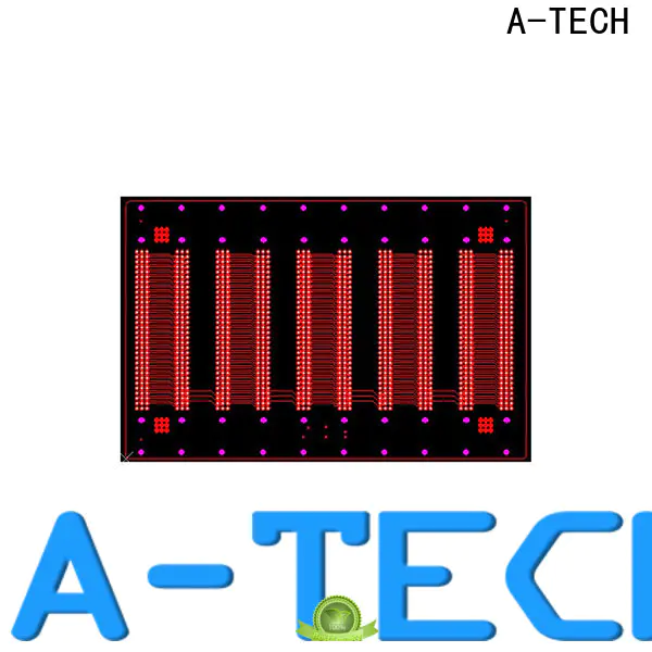
Press fit hole PCB, or called press fit pins PCB, they’re component holes with copper plated through and with tighter tolerance than standard PTH, the tolerance of standard PTH is +/-0.075mm(3mil), but the tolerance of press fit hole is normally +/-0.05mm(2mil).

Press fit holes are used as holes to fit the leads of connectors that will not be soldered but pressed into the holes. In order to accommodate lead and hole to tightly fit together, the tolerance on both are well defined, the typical tolerances for the press fit holes depends on the type of connector that is used and it’s the connector manufacturer who specifies this.

Press fit technology reduces PCB assembly time and effort considerably, and press fit pin eliminates the need for soldering, this cuts process time and cost, and boosts production output capacity. With no need to solder modules, engineers enjoy great flexibility in design. The module can easily be mounted on top or bottom of the PCB at no extra cost and effort.

A-TECH drill press fit holes with new drill bits and control specially in manufacturing process to ensure finished hole size within tolerance as specified.


Company Features
1. A-TECH CIRCUITS Co., Ltd. is a professional factory that can provide a large number of press fit pins pcb. A-TECH CIRCUITS Co., Ltd. produces pcb edge plating process in a scientific management model.
2. Listing technology as a main focus in A-TECH proves to be really efficient.
3. A-TECH CIRCUITS Co., Ltd. has accumulated a wealth of professional design experience. Consistently developing first-class via in pad with our wisdom and power is our guiding policy. Inquire now!
The creation of A-TECH via in pad focused on origin, health, safety and environmental impact. Therefore, these materials have very low Volatile Organic Compounds. The product can find its application values in the fields of electronics, lamps, printing, toy and food
There are many factors being considered while designing A-TECH press fit pins pcb. They are the selection of materials, modes of loading, safety factors, allowable stresses, etc. It is easy to store as the product is lightweight and compact
A-TECH press fit pins pcb will go through serious quality inspection. It will be randomly checked in terms of fabrics quality, strength, colorfastness, printing quality, and sewing quality. The product is made of non-toxic and odourless materials
The manufacture of A-TECH press fit pins pcb is of sophistication. It follows some basic steps to some extent, including CAD design, drawing confirmation, material selection, cutting, drilling, shaping, painting, and assembly. It can be cut and divided according to the specifications required by customers
The design of A-TECH via in pad follows these steps. They include the determination of forces acting on and energy transmitted by each element; selection of materials; confirmation of size and shape, etc. The product has good diffusivity to point light source
pcb edge plating process The variety is excellent and pure, the meat is compact and thick, the taste is tender and juicy, rich in protein, calcium, iron, zinc and other nutrients, pure natural and zero additives, safe to eat, and widely acclaimed in the market.
Product Message
Chat Online 编辑模式下无法使用
Chat Online inputting...
Please hold on and we will get back to you soon