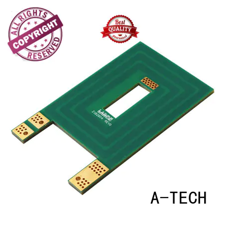
Company Advantages1. In terms of design style, A-TECH
impedance pcb has been praised by experts in the industry, for its reasonable structure and appealing appearance.
2. via in pad pcb breaks through the limitations of impedance pcb which creates a new world of press fit pins pcb .
3. A-TECH CIRCUITS Co., Ltd. has a strong sales network.
Thick copper PCB or called Heavy copper PCB, it refers to the printed circuit boards with copper thickness more than 3oz(ounce), they’re usually used for various electronic devices like central power system and power electronic devices which need high power or current through.
The applications of thick copper PCBs
● UPS systems
● Protection relays
● High power rectifiers
● Power grid switching systems
● Energy storage and power grid back up
● High power distribution
● Heat dissipation
● Planar transformers
● Power convertors
The advantages of thick copper PCB
● Better current carrying capacity
● Increased endurance to thermal strains
● Added copper plating in the heat vias
● Elimination of complex wired buss configurations
● Increased mechanical strength at connector sites
● Optimized use of exotic high temperature materials with lower probability of circuit failure
A-TECH have manufactured heavy copper PCBs more than ten years with very rich experience. Currently we’re capable of manufacturing thick copper PCB up to 12oz with our limit production capability.
Company Features1. With strong developing and manufacturing abilities of impedance pcb , A-TECH CIRCUITS Co., Ltd. has won an honorable reputation in the domestic market.
2. Besides the professionals, the progressive technology is also critical to the production of via in pad pcb .
3. We have a simple but clear purpose – to make sustainable living commonplace. We believe this is the best long-term way for our business to grow. Please contact. We always adhere to the principle of 'quality first'. Good quality products will help us win more customer. Hence, we will conduct specialized education and technical training to the workers, and work together to improve product quality. We take full responsibility for our impact on the environment, and therefore not only do we constantly strive to reduce any such impact in the course of our operations but also consistently adhere to the legal regulations governing environmental protection. Please contact. Our mission is to exceed our client’s expectations while addressing their needs and providing professional services. We also implement the most effective countermeasures to help their success.
