loading

A-TECH  >  AI - Page Sitemap  >  A-TECH flex microwave rf pcb multi-layer for led
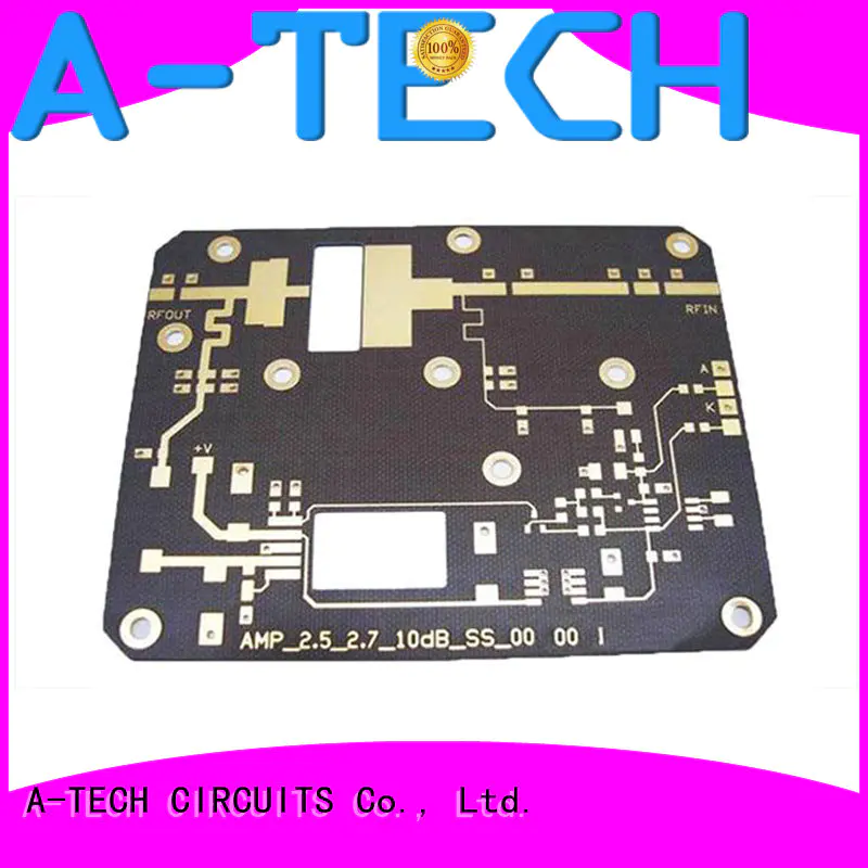
A-TECH flex microwave rf pcb multi-layer for led

A-TECH flex microwave rf pcb multi-layer for led

Layer
2
Material
Taconic RF35
Min Order Quantity
No
Production Lead Time
4-15 Working Days
Supply Capacity
2000 ㎡/Month
Certifications
UL, ISO9001, TS16949
Payment Terms
T/T, Paypal, WU etc.
Shipment Terms
EXW, FOB, DDU etc.
Test Way
100% E-Test
Standard
IPC CLASS 2 / CLASS 3
Price
Get Latest Price
Get the latest price
Quantity Needed:
Pieces
E-mail:
Product Comparison
Compared with same kind of products in the industry, PCB prototype has the following highlights due to the better technical capability.
Company Advantages
1. A-TECH microwave rf pcb is developed using latest technology support.
2. This product has the required safety. We have assessed and eliminate potential hazards by using the principles detailed in EN ISO 12100:2010.
3. Thanks to its energy efficiency, the product not only has a positive impact on the environment but it also greatly reduces people's energy bills.
4. This product will only need a lesser replacement and maintenance, so people can assure that it can contribute to saving money and time as well.


Microwave RF PCB, it’s also known as high frequent PCB, they use materials of excellent dielectric property for its main body with other dielectric materials and metal substrates matched to complete corresponding multi-layer processing or thick-film processing and manufacture and to achieve the transmission functions of excellent high thermal conductivity, low dielectric constant, high frequency and high speed.


The features of Microwave RF PCB

● The thermal expansivity should be the same with copper foil as much as possible, because the difference will lead toe copper foil separated in the changes of cold and heat.
● Heat resisting property, chemistry resisting, impact endurance, peel off resisting must be good.
● Water absorptivity must be low, high water absorptivity will affect DK and DF when in the wet environment
● DK should be small and stable enough, usually the smaller the better, high DK may lead to signal transmission delay
● DF should be small, which mainly affect quality of signal transmission, the smaller DF could make smaller signal wastage accordingly


The applications of Microwave RF PCB

● Microwave transmission
● Automobile telephone
● Wireless networks
● Wireless communications
● Satellite microwave communications
● 4G & 5G networks


A-TECH CIRCUITS have increased investment and intensity of research & development on Microwave high frequency PCB over the last few years to meet the continuously increasing demands. We have obtained rich knowledge and experience in professional manufacturing of various high-frequency PCBs from prototypes to production run. For main RF PCBs, such as Teflon PCB, Rogers PCB, Taconic PCB and Arlon PCB, we have sufficient inventory to ensure fast delivery.


General specification for Microwave/RF PCB in A-TECH
Layer Count1-6
Board thickness0.4-3.2mm
Copper thickness0.5-3oz
Dielectric Constant(DK)2.2-10.3
Min trace width/spacing4/4mil
Min drill hole size0.2mm
Surface treatmentHAL(Lead free), Immersion Gold/Tin/Silver, OSP, Gold Plating.
Material availableTeflon, Rogers, Taconic, Arlon, etc


Company Features
1. After years of development, A-TECH CIRCUITS Co., Ltd. has become a reliable supplier and manufacturer of microwave rf pcb .
2. Strong technical capabilities make A-TECH CIRCUITS Co., Ltd. stand at the forefront of the multilayer pcb industry.
3. A-TECH CIRCUITS Co., Ltd. actively contributes to the industry, be proud of the work, and be proud of the achievements. Call! New standards will continue to be created through A-TECH CIRCUITS Co., Ltd.'s innovations. Call! A-TECH CIRCUITS Co., Ltd. aims to create a new brand for single-sided PCB and create a new market space. Call! A-TECH adheres to the concept of putting customers first. Call!
single-sided PCB Selected high-quality raw materials, manufactured with exquisite craftsmanship, has good air permeability, strong practicability, and good decorative effect, and is well received in the market.
multilayer pcb manufacturing is a children's play equipment that integrates amusement, sports, intelligence, fitness and other functions. It is designed for children who like drilling, climbing, sliding, swinging, jumping, shaking, etc., and can exercise children's guts very well. and courage.
multilayer pcb manufacturing The double-layer sealing design can reduce the volatilization of moisture in the wet wipes, keep the wet wipes in the bag moist for a long time, and will not dry for a long time.
multilayer pcb The design is simple and stylish, the workmanship is exquisite and delicate, the shape is beautiful and generous, the quality is safe and reliable, and it is both beautiful and practical. It is your ideal LED lamp shell product.
multilayer pcbSimple design, stylish shape, excellent material selection, fine workmanship, reliable quality and durability, it is your quality choice.
The product stands out for its anti-fungal property. The formulas of this product contain antibacterial ingredients that do no harm to the skin.
Product Message
Chat Online 编辑模式下无法使用
Chat Online inputting...
Please hold on and we will get back to you soon