loading

A-TECH  >  AI - Page Sitemap  >  A-TECH fit hole hybrid pcb hot-sale top supplier
A-TECH fit hole hybrid pcb hot-sale top supplier

A-TECH fit hole hybrid pcb hot-sale top supplier

Type of Blind Vias
Laser Drill & Mechanical Drill
Min Laser drill blind Vias
0.1mm
Min Mechanical drill blind vias
0.15mm
Min Buried Vias
0.15mm
Min Order Quantity
No
Production Lead Time
6-20 Working Days
Supply Capacity
3000 ㎡/Month
Certifications
UL, ISO9001, TS16949
Payment Terms
T/T, Paypal, WU etc
Shipment Terms
EXW, FOB, DDU etc.
Test Way
100% E-Test
Standard
IPC CLASS 2 / CLASS 3
Price
Get Latest Price
Get the latest price
Quantity Needed:
Pieces
E-mail:
Company Advantages
1. A-TECH CIRCUITS Co., Ltd. values the quality and safety of material. It is extremely popular in the markets of Europe, North America, and Asia
2. Some customers said they chose this product mainly for the purpose of conspicuously and unconsciously make their brand known to the public and attract potential customers. The product is certified under UL(E357001) and RoHS
3. hybrid pcb is manufactured carefully based on high-quality materials. It is firm and durable with quality excellence. It is not easy to get dirty and yellow as well as to crack.


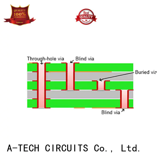
PCB with Blind and Buried Vias

Basically the blind and buried vias are popular to be designed on high density PCBs due to the limit of small space, the blind and buried vias can only pass through necessary layers and more surface area become available for components, they have the ability to meet the density constraints of line and pads on a typical design without increasing the layer count or board size and reduce the PCB aspect ratio for convenient production.


Blind Vias

Blind via is a copper plated hole that connects only one outer layer to one or more inner layers, it never goes all the way through a circuit board but only visible on one side of circuit boards. The blind via can be laser or mechanically drilled based on the detailed via hole size and layer stackup.


Buried Vias

Buried Via is a copper plated hole that connects two or more inner layers without contacting the outer layers, as the name suggests, it’s buried inside, so it’s not visible from the outer layer of PCB. Buried via has no impact to any trace or surface mount component on the top or bottom layers, trace or SMD pad can be placed directly over the buried via.

A-TECH CIRCUITS has capacity to build both of blind via and buried via with different demands, We’ll use laser drill for the blind vias with size smaller than 150um and use mechanical drill for the blind via size larger than 150um, the technology of blind via we can achieve include via in pad, stacked via and staggered via. The minimum size of buried via normally need to be 150um and they’ll be plugged with resin to avoid prepreg flow into buried via which might affect the connection with adjacent layers.


Company Features
1. A-TECH CIRCUITS Co., Ltd. has many veteran technicians to offer customers technical support for hybrid pcb.
2. All our members are working hard to build the first brand of edge plating pcb castellation . Get quote!
The development of A-TECH edge plating pcb castellation has adopted many high tech. They are mainly electronic information technology, automatic control theory, and microtechnology. This product has been certified under FCC, CE, PSE, and RoHS
The mechanical components of A-TECH edge plating pcb castellation are precisely manufactured. Various kinds of CNC machines are used such as the cutting machine, drilling machine, milling machine, and punching machine. This product features high-speed endurance and compatibility
The manufacture of A-TECH edge plating pcb castellation is of professionalism. The multistage production process is adopted. Its design, production, assembly, and testing will be controlled by separate teams. This product is in compliance with the standards of the European Union Association and the HDMI Association of the United States
A-TECH hybrid pcb is well designed. Its detailed design includes mechanical design, structural design, electrical control design, instrument panel design, etc. With the help of a special adapter, the product can be converted into other types of cable
A-TECH edge plating pcb castellation is manufactured using a variety of high technologies. They are mainly sensing technology, control system, detection system, and servo drive technology. This product has been certified under FCC, CE, PSE, and RoHS
The product has better durability due to its quality assurance. This product is able to deliver a high-quality and stable digital signal
Product Message
Chat Online 编辑模式下无法使用
Chat Online inputting...
Please hold on and we will get back to you soon