loading

A-TECH  >  AI - Page Sitemap  >  A-TECH fit hole edge plating pcb best price for sale
A-TECH fit hole edge plating pcb best price for sale

A-TECH fit hole edge plating pcb best price for sale

Depth of routing
Customized
Tolerance of routing
+/-0.1mm
Min Order Quantity
No
Production Lead Time
6-18 Working Days
Supply Capacity
2000 ㎡/Month
Certifications
UL, ISO9001, TS16949
Payment Terms
T/T, Paypal, WU etc.
Shipment Terms
EXW, FOB, DDU etc.
Test Way
100% E-Test
Standard
IPC CLASS 2 / CLASS 3
Price
Get Latest Price
Get the latest price
Quantity Needed:
Pieces
E-mail:
Product Comparison
Compared with other products in the same category, Aluminum PCB has outstanding advantages which are mainly reflected in the following points.
  • v s
Enterprise Strength
  • A-TECH always gives priority to customers and services. We continuously provide excellent services for numerous customers.
Company Advantages
1. You can choose to design by yourselves for our edge plating pcb .
2. This product stands out for its breathability. Its materials used provide a ventilated environment that would not allow the heat and moisture to accumulate.
3. A-TECH CIRCUITS Co., Ltd. has made in-depth adjustments to the organizational structure, brand, and production layout.


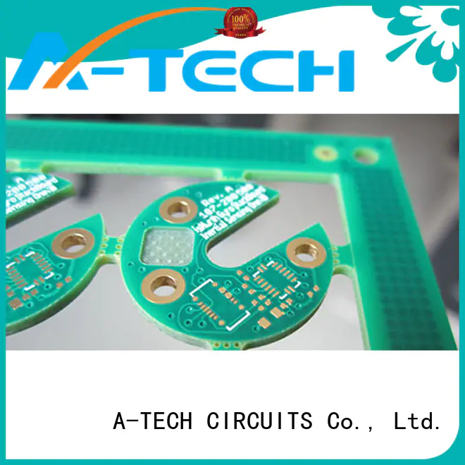
Depth control routing(milling) is also known as Z-axis milling or level milling, it refers to partial routing in printed circuit board manufacturing with a variable level elevation at the PCB edge or within PCB.

Control depth routing technology supports a high end market with the need for accuracy, miniaturization, process stability and the need for productivity, and depth routing option allows for very complex designs, bended boards and structures to be processed with fine precision.

Depth control routing technology have great advantages in PCB assembly as the special shape of depth routing.



A-TECH fit hole edge plating pcb best price for sale-1

● It can avoid cold soldering as siphonic effect use NPTH step stair slot
● Use the step stair in middle of PCB apply in special module application, and degrade the height of PCB assembly, achieve refinement and miniaturization
● Use the step stair of PCB edge make card slot is favor for PCB fixed and installation
● Use Special size NPTH step stair as resonant cavity of microwave signal, degrade signal loss and other special function.


A-TECH has manufacturing capability to build various types of depth routing with different size and depth, no matter on the PCB edge or within the PCB, and the precision tolerance can be controlled as +/-0.1mm(4mil).


Company Features
1. A-TECH CIRCUITS Co., Ltd. is a leader in the world of edge plating pcb industry.
2. A-TECH has advanced technology to be implemented in the production of via in pad pcb .
3. We conduct our business in line with the highest ethical and operational standards. We focus on activities that deliver added value to partners and customers. We strictly take steps to formalize our environmental practices. We work to foster a sustainable development along our entire value chain in line with our economic, environmental and social responsibilities. We adopt eco-friendly manufacturing approach to promote sustainability. We have replaced some aging manufacturing equipment with energy-saving ones, such as electricity-saving equipment to help cut down electricity consumption. We have invested efforts in sustainability throughout the entire business operations. From raw materials procurement, workmanship, to packaging methods, we comply with relevant environmental regulations.
A series of tests for A-TECH via in pad pcb have been carried out. It has strictly tested in terms of the performance of the circuit board, plugs, voltage, housing, etc. Using high quality cables, the product features great conductivity
A-TECH via in pad pcb go through a polishing process once it is processed by CNC machines. It is gauged, calibrated and then polished to a perfect finish in a wide range of colors and designs. The product has been certified under CE, FCC, UL, and BS
A-TECH via in pad pcb has a good design. Its elements are programmed to respond to climatic factors, to improve energy efficiency or reduce solar heat, or for aesthetic reasons such as an art installation. The product can effectively output fixed voltage
The workmanship of A-TECH via in pad pcb carefully conducted. It should go through timber cutting, tenoning, trepanning, pressing, or high-speed milling processes. With wide compatibility, the product works perfectly with other devices
The package of A-TECH via in pad pcb will be done with professional materials. It is packaged with hardened carton, foam, cardboard, or wooden box to protect it in an all-around way to minimize transportation damage. The product can effectively provide the ultimate protection for the devices
impedance calculator pcb is equipped with an advanced heat exchanger to greatly improve the heat exchange efficiency of the evaporator. Moreover, it has a variety of protection functions. It is of good durability and reliable safety.
Product Message
Chat Online 编辑模式下无法使用
Chat Online inputting...
Please hold on and we will get back to you soon