loading

A-TECH  >  AI - Page Sitemap  >  A-TECH buried via in pad pcb best price for wholesale
A-TECH buried via in pad pcb best price for wholesale

A-TECH buried via in pad pcb best price for wholesale

Max copper thickness
12oz
Min Order Quantity
No
Production Lead Time
4-15 Working Days
Supply Capacity
5000 ㎡/Month
Certifications
UL, ISO9001, TS16949
Payment Terms
T/T, Paypal, WU etc.
Shipment Terms
EXW, FOB, DDU etc.
Test Way
100% E-Test
Standard
IPC CLASS 2 / CLASS 3
Price
Get Latest Price
Get the latest price
Quantity Needed:
Pieces
E-mail:
Product Comparison
Compared with similar products, A-TECH's PCB prototype has the following advantages.
  • v s
Company Advantages
1. The surface treatment of A-TECH via in pad pcb consists of several stages, including rust, grease, and oxidization resistant treating processes. All these processes are carefully done to guarantee its resistant capacity.
2. The product has the desired reliability. It is equipped with an intelligent circuit breaker that features reliability and accuracy, ensuring it can work without failure.
3. As the product is more economical and practical than similar products in the industry, it will be more widely used.
4. This product is reliable in property and reputably appraised by customers in the industry.


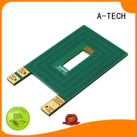
Thick copper PCB or called Heavy copper PCB, it refers to the printed circuit boards with copper thickness more than 3oz(ounce), they’re usually used for various electronic devices like central power system and power electronic devices which need high power or current through.


The applications of thick copper PCBs

● UPS systems
● Protection relays
● High power rectifiers
● Power grid switching systems
● Energy storage and power grid back up
● High power distribution
● Heat dissipation
● Planar transformers
● Power convertors


The advantages of thick copper PCB

● Better current carrying capacity
● Increased endurance to thermal strains
● Added copper plating in the heat vias
● Elimination of complex wired buss configurations
● Increased mechanical strength at connector sites
● Optimized use of exotic high temperature materials with lower probability of circuit failure


A-TECH have manufactured heavy copper PCBs more than ten years with very rich experience. Currently we’re capable of manufacturing thick copper PCB up to 12oz with our limit production capability.


Company Features
1. A-TECH has ranked top in via in pad pcb manufacture industry.
2. A-TECH heavy copper pcb is produced with the latest technology.
3. We regularly ask our stakeholders for comment and feedback on our sustainability program. We work towards our targets over the year and monitor our progress quarterly to make sure that we are meeting them. We care about the community, the planet, and our future. We are committed to protecting our environment by executing strict production plans. We are putting every possible effort in reducing negative production impact on the earth.
This kind of heavy copper pcb is practical and economical for the needs of heavy copper pcb. The product has a good barrier effect on moisture, bacteria, and dust
The principal part of via in pad pcb is made by advanced via in pad pcb. The product is widely used in the agricultural, medical and furniture field
In order to strictly control quality, A-TECH CIRCUITS Co., Ltd. selects heavy copper pcb as raw material. Its flexibility makes it easy to be molded into a variety of shapes
Different from common material, material for via in pad pcb gains the absolute advantage in characteristics of via in pad pcb. The product is a new generation of environmentally friendly material
Dissipation factor is small for via in pad pcb. The product has a good barrier effect on moisture, bacteria, and dust
The product stands out for its good heat dissipation. Built-in latest cooling system with adequate airflow, it can work or stand by for a long time. The product is both reusable and recyclable
Product Message
Chat Online 编辑模式下无法使用
Chat Online inputting...
Please hold on and we will get back to you soon