loading

A-TECH  >  AI - Page Sitemap  >  A-TECH buried via in pad pcb best price for sale
A-TECH buried via in pad pcb best price for sale

A-TECH buried via in pad pcb best price for sale

Layer
6
Material
FR4 + RO4350B
Min Order Quantity
No
Production Lead Time
10-20 Working Days
Supply Capacity
2000 ㎡/Month
Certifications
UL, ISO9001, TS16949
Payment Terms
T/T, Paypal, WU etc.
Shipment Terms
EXW, FOB, DDU etc.
Test Way
100% E-Test
Standard
IPC CLASS 2 / CLASS 3
Price
Get Latest Price
Get the latest price
Quantity Needed:
Pieces
E-mail:
Application Scope
PCB prototype developed and produced by our company can be widely used in various industries and professional fields.A-TECH is committed to providing customers with high-quality PCB prototype as well as one-stop, comprehensive and efficient solutions.
Product Comparison
A-TECH's PCB prototype has more advantages over similar products in terms of technology and quality.
  • v s
Company Advantages
1. The quality control of A-TECH 2oz copper pcb is conducted rigorously. It has been certified under relevant pool standards, such as ANSI, APSP, and UL.
2. via in pad pcb endows with excellent technique and stable quality.
3. 'I was tentative to make such a big financial investment in my health, but I’m so glad I did. The product has been transformative.' - One of our customers says.

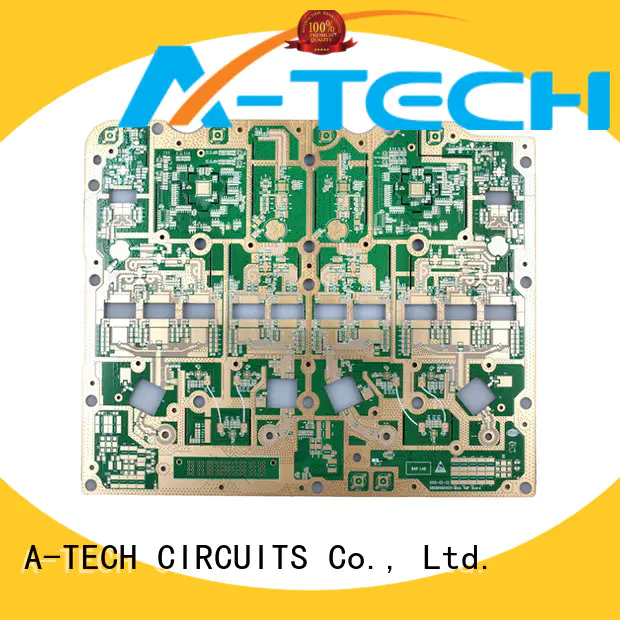
Hybrid PCB is also known as mixed material lamination, it’s normally combined by two different material like FR4 and PI(rigid flex PCB), FR4 and Ceramic, FR4 and Teflon, FR4 and Aluminum base etc.


The challenge to manufacture the Hybrid PCB is managing the different coefficient of thermal expansion properties of the dissimilar circuit materials both during PCB manufacturing and component assembly.


Hybrid PCB with a combination of FR4 material and PTFE material allows a designer to condense both RF functionality and RF functionality on the same PCB which can reduce both the footprint of the device and the cost.


When producing a printed circuit board with dissimilar materials it’s critically important to have experience in both the physical properties of the laminate and the capabilities of your equipment. Based upon the CTE values of all of the layers of material(ex FR4, PTFE and Copper), each material grows at a different rate during elevated thermal exposure. This can cause significant registration issues as one material shrinks while another one expands and it can also cause delamination of the copper-to substrate interfaces. Therefore, not all materials should be used in hybrid applications as they are not manufacturable regardless of the desired performance.


Hybrid constructions typically involve a low loss material such as Nelco or Rogers combined with another core material like FR4, the details include FR4 and Rogers4350B, FR4 and Rogers 4003C, FR4 and Aluminum base etc.


Company Features
1. We have experience in manufacturing 2oz copper pcb .
2. Strictly following the quality management system more guarantees the distinguished performance of via in pad pcb .
3. A-TECH CIRCUITS Co., Ltd. pays great attention to the reputation of its own brand. Please contact us! A-TECH CIRCUITS Co., Ltd.'s mission is to provide high-value products and services on global scale. Please contact us!
A-TECH via in pad pcb undergoes a series of the strict assessment process which includes flammability tests, rain resistance test, ventilation test, and marking and labeling guidelines.
All of the mechanical components of A-TECH 2oz copper pcb are manufactured under sophisticated workmanship. The workmanship includes material preparation, material cleaning, cutting, stamping, spraying, and surface treating.
The manufacture of A-TECH 2oz copper pcb is of professionalism. The multistage production process is adopted. Its design, production, assembly, and testing will be controlled by separate teams.
The workmanship of A-TECH 2oz copper pcb carefully conducted. It should go through timber cutting, tenoning, trepanning, pressing, or high-speed milling processes.
A-TECH via in pad pcb has been tested. It is tested and certified by the National Sanitation for Food Safety and Food Contact under the NSF 51 Certification.
To design 2oz copper pcb should follow such principles which are: via in pad pcb.
Product Message
Chat Online 编辑模式下无法使用
Chat Online inputting...
Please hold on and we will get back to you soon