loading

A-TECH  >  AI - Page Sitemap  >  A-TECH blind blind vias pcb company at discount
A-TECH blind blind vias pcb company at discount

A-TECH blind blind vias pcb company at discount

Min half hole
0.55mm
Profile of half hole
Routing
Surface finish
ENIG preferred
Min Order Quantity
No
Production Lead Time
5-18 Working Days
Supply Capacity
10000 ㎡/Month
Certifications
UL, ISO9001, TS16949
Payment Terms
T/T, Paypal, WU etc.
Shipment Terms
EXW, FOB, DDU etc.
Test Way
100% E-Test
Standard
IPC CLASS 2 / CLASS 3
Price
Get Latest Price
Get the latest price
Quantity Needed:
Pieces
E-mail:


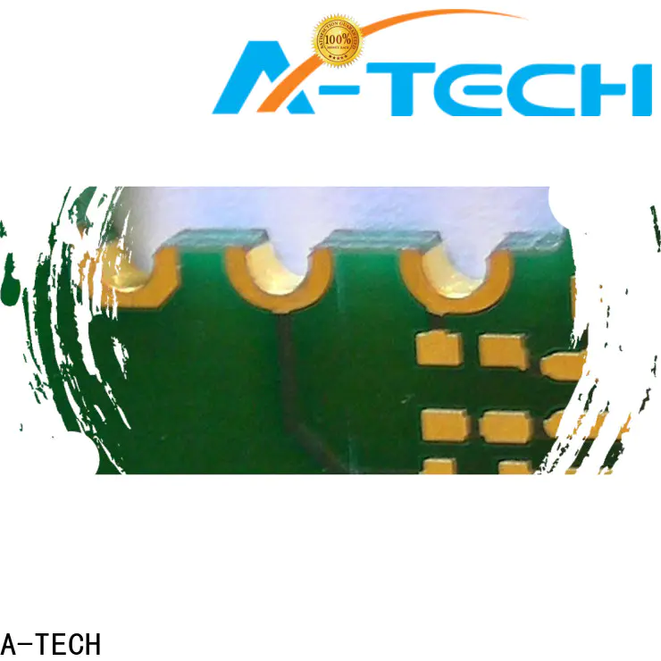
Plated half holes which is also called castellated holes, they’re normally designed at the edge of printed circuit boards and plated with copper, and they’re mainly used for board-on board connections, mostly where two circuit boards with different technologies are combined.

Most of the plated half hole PCBs are a type of modules which are small and high density with fine pitch components, this type of circuit boards are made with GPS Modules, Wifi Modules, Bluetooth Modules, GMS Modules, GPRS Modules and other smart modules.

Basically plated half holes are not suitable for V-score process, because the copper at the hole will be rolled up to cause serious burs, routing process is a better solution to ensure smooth edge.


The guidelines of designing plated half holes

● Normally the minimum half hole size is 0.8mm, it can be min 0.55mm with A-TECH capability
● The routing tolerance for half hole is +/-0.15mm
● The minimum distance from pad to pad is 0.25mm
● Use the larger hole diameter if possible
● Use the larger outer layer pad on both sides if possible
● Connect inner layer pads to the plated holes if possible to bring more stability and help to avoid burrs.
● Routing process is preferred and ENIG finish is preferred.


A-TECH have manufactured a large number of printed circuit boards with half hole design for various module products, and we have obtained rich experience to control high quality, the minimum half hole size we can build is 0.55mm.


A-TECH blind vias pcb adopts the smooth and high-efficiency manufacturing process. It gains much recognition in overseas markets, including Southeast Asia, Europe, Africa, and America
A-TECH blind vias pcb is delicately crafted by our adept professionals by using modern technology. The product is certified under CE and passes FDA and SGS tests
A-TECH blind vias pcb is designed and crafted using premium quality basic material. It gains much recognition in overseas markets, including Southeast Asia, Europe, Africa, and America
Our expert's extensive knowledge of the various materials ensures the A-TECH blind vias pcb is made of the most appropriate materials. Its PLC screen is characterized by high sensitivity to orders
A-TECH blind vias pcb is manufactured from optimum quality raw materials that render superior durability. The focused laser beam is capable of accurately evaporating objects or dirt from the processed item
A-TECH CIRCUITS Co., Ltd.Through continuous technological learning and innovation, new concepts are incorporated into the R&D and production of press fit pins pcb, and the traditional model is broken through. Its own scientific cost control measures make the price of the product better, so that the overall cost performance of the product is higher, and it has more advantages in the market competition.
Product Message
Chat Online 编辑模式下无法使用
Chat Online inputting...
Please hold on and we will get back to you soon