Latest products
What are the anti-interference measures for PCB circuits?
by:A-TECH
2021-03-12
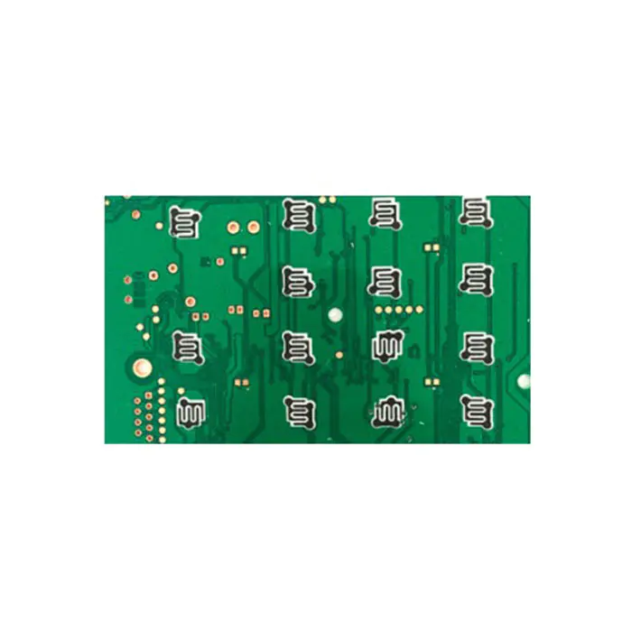
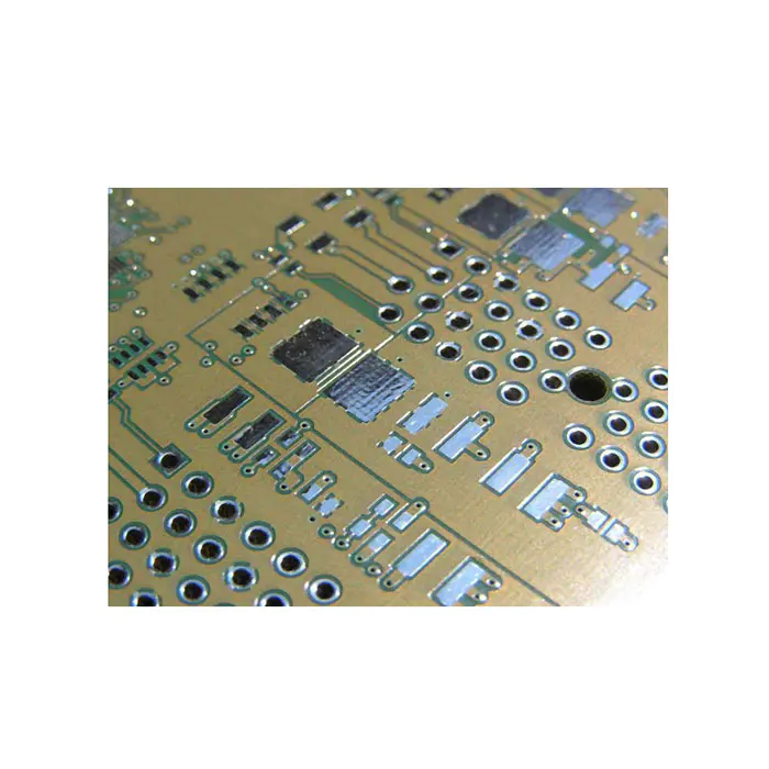
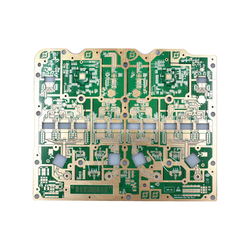
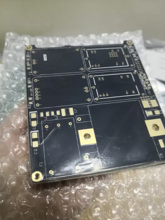
With the development of social economy, my country's science and technology have developed rapidly and achieved unprecedented results. However, electronic information systems are the products of science and technology and are widely used in all walks of life. When it comes to electronic information technology, the topic of electromagnetic interference is inevitable, because electromagnetic interference will reduce the effective performance of electronic equipment during actual use. Secondly, the anti-interference of printed circuit boards is closely related to specific circuits. Here I will explain to you the common measures of PCB anti-interference design. 1. The principle of ground wire design; if there are both logic circuits and linear circuits on the circuit board, they should be separated as much as possible. The ground of the low-frequency circuit should be grounded in parallel with a single point as much as possible. If the actual wiring is difficult, it can be partially connected in series and then connected in parallel. Grounded. 2. The grounding wire forms a closed loop; the printed circuit board is composed of only digital circuits, and the grounding circuit is arranged into a loop, which can improve the anti-noise ability. 3. On the premise that the speed can meet the requirements, try to reduce the crystal oscillator of the single-chip microcomputer and select low-speed digital circuits. 4. IC devices should be soldered directly on the circuit board as much as possible, and IC sockets should be used less. To make the electronic circuit get better performance, the layout of the components and the design layout of the wires must be just right. In addition to the above commonly used measures, we must take into account the size of each PCB. What to do if the PCB size is too large, the printed lines are long, the impedance increases, the anti-noise ability is reduced, and the cost also increases; if the PCB size is too small, it means that the heat dissipation is not good, and the adjacent lines are susceptible to interference. After determining the PCB size, determine the location of the special components. Finally, according to the function of the circuit, it is the best choice to lay out all the components of the circuit. PCB has always insisted on using superb technical force, sophisticated production equipment, perfect testing methods, product quality higher than industry standards, and warm and thoughtful service, which has won praise and welcome from global merchants and users.
Custom message