Latest products
Spacing between patches
by:A-TECH
2020-04-18
The spacing between patch components is a problem that engineers must pay attention to. If the spacing is too small, it is very difficult to print solder paste and avoid soldering tin.
The distance suggestions are as follows: Device distance requirements between patches: similar devices: ≥ 0. 3mm heterogeneous devices: ≥ 0. 13 * h 0. 3mm (H is the maximum height difference of neighboring components)
The distance between components that can only be manually pasted requires: ≥ 1. 5mm.
The above suggestions are for reference only and can be in accordance with the PCB process design specifications of their respective companies.
2. The distance between the in-line device and the patch, as shown above, should be kept sufficient distance between the in-line resistor device and the patch. It is recommended to be 1-Between 3mm.
Due to the troublesome processing, the use of direct plug-ins is now rare.
3. For the placement of decoupling capacitors of IC, decoupling capacitors need to be placed near the power port of each IC, and the position should be as close as possible to the power port of IC.
When a chip has multiple power ports, decoupling capacitors should be arranged at each port.
4. The placement direction and distance of components at the edge of PCB board are generally made of jigsaw boards, so the devices near the edge need to meet two conditions: 1. Parallel to the cutting direction, make the mechanical stress of the device uniform.
If it is placed in the way on the left side of the figure above, when the jigsaw puzzle is to be split, the two pads of the patch may fall off due to different stress directions.
2. Devices cannot be arranged within a certain distance to prevent components from being damaged when the board is cut.
5. When adjacent pads need to be connected, if adjacent pads need to be connected, first confirm to connect outside to prevent bridging caused by connecting into a group, and pay attention to the width of copper wire at this time.
6. If the pad falls in the common area, heat dissipation should be considered. If the pad falls in the paving area, the right way should be adopted to connect the pad with the paving, in addition, it is determined whether to connect 1 wire or 4 wires according to the current magnitude;
If the left way is adopted, it is difficult to weld or repair and disassemble components, because the temperature is completely dispersed by the copper paved, resulting in failure to weld.
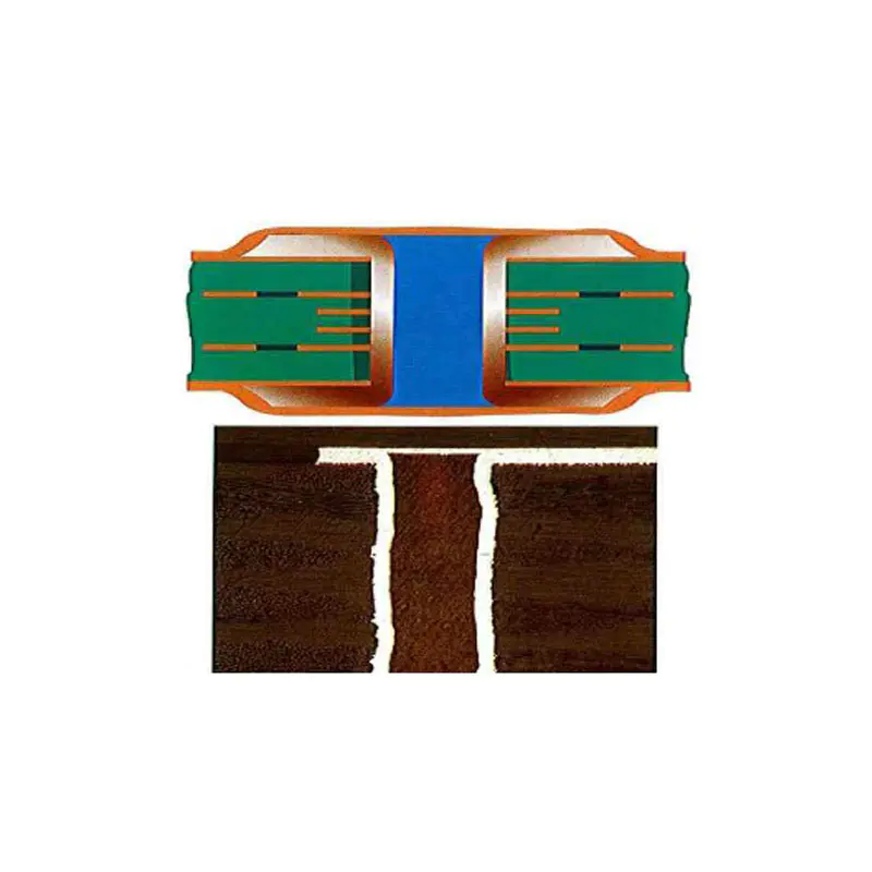
7. If the lead wire is smaller than the plug-in pad, tears need to be added. If the lead wire is smaller than the pad of the in-line device, tears need to be added (As shown above).
Adding Teardrops has the following advantages: 1. Avoid reflection caused by sudden decrease of signal line width, which can make the connection between the trace and the component pad tend to smooth transition.
2. The problem that the connection between the PAD and the trace is easily broken by the impact force is solved.
3. Setting tears can also make the PCB circuit board look more beautiful.
8. The lead widths on both sides of the component pad should be the same. As shown in the above figure, the lead widths on both sides of the component pad should be the same.
9. Pay attention to keep the pads of unused pins and ground. Pay attention to keep the pads of unused pins and ground correctly.
For example, in the above figure, a chip has two pins that are not used, but the physical pins of the chip exist.
If the two pins are suspended as shown on the right side of the figure above, it is easy to cause interference.
If the pad is added and the pad is grounded, interference can be avoided.
10, the through hole is best not to hit on the pad, pay attention to the through hole is best not to hit on the pad, easy to cause leakage tin solder.
11. Pay attention to the distance between the wires or components and the board edge. It is worth noting that the leads or components cannot be too close to the board edge, especially the single panel. The general single panel is mostly paper plate, which is easy to break after being stressed, if the components are connected or placed at the edge, they will be affected.
12. The ambient temperature of the electrolytic capacitor must be considered. To keep away from the heat source, first consider whether the ambient temperature of the electrolytic capacitor meets the requirements. Secondly, keep the capacitor away from the heating area as far as possible, in case the liquid electrolyte inside the electrolytic capacitor is baked dry.
Custom message