
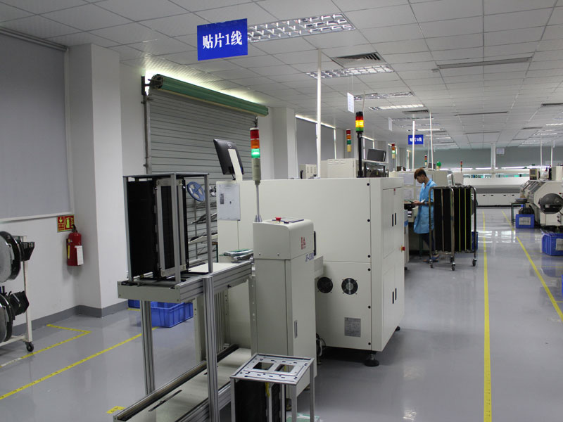
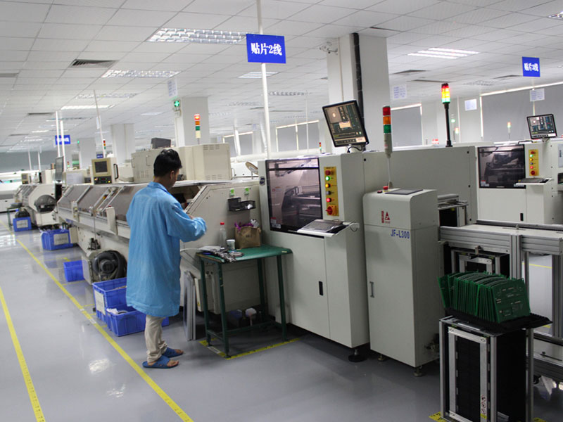
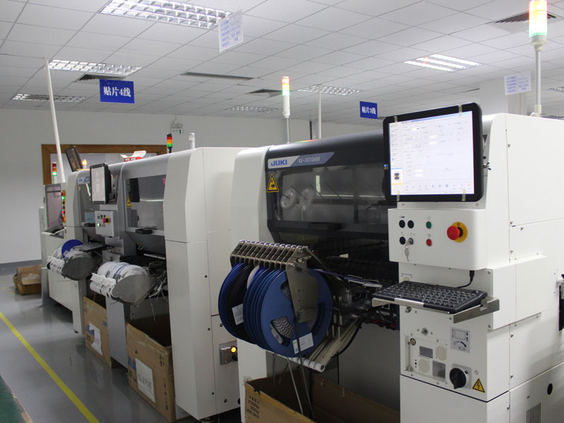
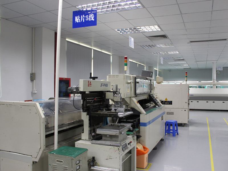
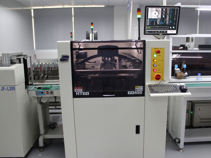
In order to meet continuously growing demands from our customers and worldwide market, A-TECH started to set up assembly lines in 2013 to provide one stop services from PCB manufacturing, components sourcing to assembly production.
The PCB Assembly Services we can offer
● Multiple PCB Assembly Service
- Full Turnkey PCB Assembly
- Partial Turnkey PCB Assembly
- Consigned PCB Assembly
● Flexible Volume Assembly
- Prototype PCB Assembly
- Small Volume PCB Assembly
- Medium Volume PCB Assembly
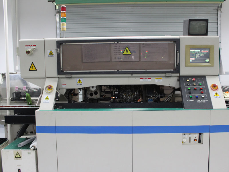
● Different Assembly Technology:
- Surface Mount Technology(SMT)
- Through Hole Technology(THT)
- Mixed Technology(SMT & THT)
- Single or Double Sided Placement
- Conformal Coating
● Various Testing & Inspection Services
- Visual Inspection
- Automated Optical Inspection(AOI)
- X-Ray Inspection
- In-Circuit-Test(ICT)
- Function Test
| No | Item | Technical data |
| 1 | Assembly Types | Surface mount Thro-hole Mixed technology(SMT & Thru-hole) Single or double sided placement Conformal coating |
| 2 | Solder Types | Lead-free - RoHS |
| 3 | Parts Procurement | Full Turnkey Partial turnkey Consigned |
| 4 | PCB board types | Rigid PCB Flexible PCB Rigid-flex PCB Metal core PCB |
| 5 | Component types | SMT 0201 or larger BGA 0.35mm pitch, POP(package on Package) <br/WLCSP 0.35mm pitch Hard metric connectors Cable & Wire |
| 6 | SMT Parts Presentation | Bulk Cut tape Partial reel Reel Tube Tray |
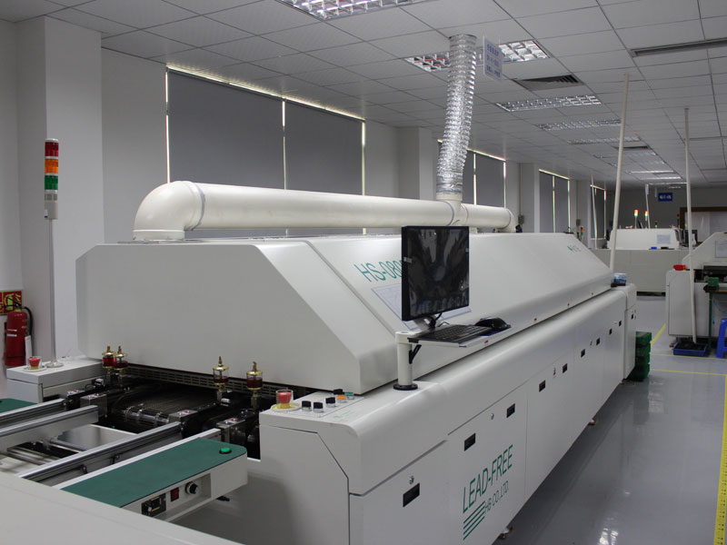
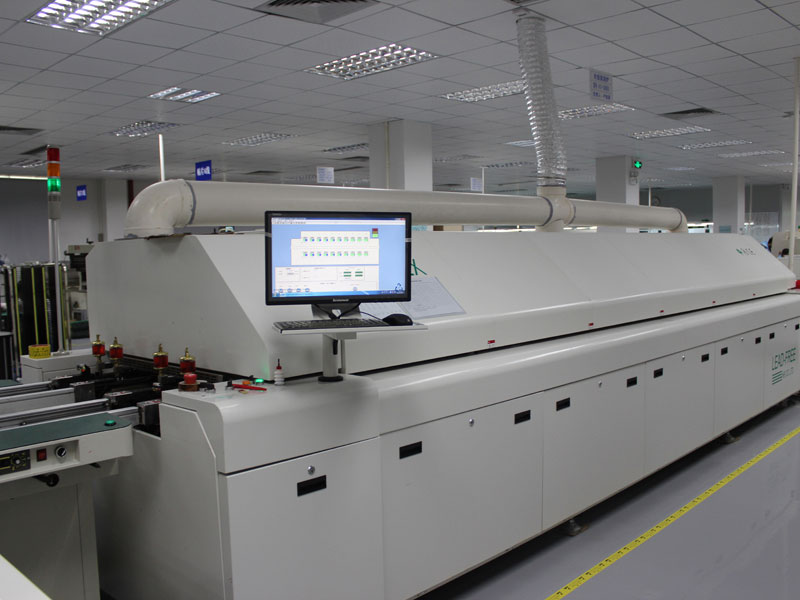
| 7 | Type of soldering | Reflow soldering Wave soldering Hand soldering |
| 8 | Testing & Inspection | Visual Inspection AOI(Automated Optical Inspection) X-Ray Inspection Function Testing |
Components Quality Control
In order to ensure good quality of components, there are several processes that we follow:
1.An overview of the visual electronic components inspection process include
1.1 Packaging examined: Weighed and checked for damage; Taping condition inspected-dented package etc; Original factory sealed vs. non-factory sealed.
1.2 Shipping documents verified: Country of origin; Purchase order and sales order numbers match;
1.3 Manufacturer P/N, quantity, date code verification, RoHS
1.4 Moisture barrier protection verified – vacuum sealed and humidity indicator with specification.
1.5 Products and packaging (photographed and cataloged)
1.6 Body marking inspection (faded markings, broken text, double print, ink stamps etc.)
1.7 Physical conditions inspection (lead bands, scratches, chipped edges etc.)
1.8 Any other visual irregularities found.
Once our visual distribution inspection is completed, products are escalated to the next level-electronic components engineering distribution inspection for review.
2.Engineering Components Inspection
Our highly skilled and trained engineers receive the components for evaluation at a microscopic level to ensure consistency and quality. Any suspect parts or discrepancies that are discovered in the visual inspection process will either be verified or discounted by taking a product sampling of the material.
The engineering electronic components distribution inspection process includes:
2.1Review visual inspection findings and notes.
2.2Purchase and sales orders numbers verified.
2.3Verification of labels(bar codes)
2.4 Manufacturer’s logo and date log verification.
2.5 Moisture sensitivity level and RoHS status.
2.6 Extensive marking permanency tests.
2.7 Review and comparision to manufacturer data sheet.
2.8 Additional photos taken and cataloged.
2.9 Solderibility Testing.
AOI Inspection for surface mount technology(SMT)
As a primary testing technique in PCB assembly, AOI applies to fast and accurate inspection of errors or defects occurring in PCB assembly process, so that high quality of PCB assemblies can be ensured with no defect after their leaving assembly line. AOI is contributive to efficiency improvement because it is placed on SMT assembly line, just after reflow. As soon as some problems are inspected and reported by AOI equipment, engineers can instantly change corresponding parameters in the previous stages of the assembly line, so that remaining products will be correctly assembled. AOI can cover primarily come in soldering and components categories. In terms of soldering, AOI detect the defects ranged from open circuits, solder bridges, solder shorts, insufficient solder to excess solder. Component defects include lifted lead, missing components, misaligned or misplaced components.
X-Ray Inspection
Our automated X-Ray inspection systems are able to monitor a variety of aspects of a printed circuit board in assembly production. The inspection is done after the soldering process to monitor defects in soldering quality. Our equipment is able to “see” solder joints that are under packages such as BGA, CSP and FLIP chips where the solder joints are hidden. This allows us to verify that the assembly is done correctly. The defects and other information detected by the inspection system can be quickly analyzed and the process altered to reduce the defects and improve the quality of the final products. In this way not only are actual faults detectd, but the process can be altered to reduce the fault levels on the boards coming through. Use of this equipment allows us to ensure that the highest standards are maintained in our assembly.
Laser Cut Stencil & Solder Paste Stencil
Laser Cut Stencils, or called Solder Paste Stencils are used to print the right amount of solder paste onto the soldering pads of PCB for SMT circuit board assembly. All solder paste stencils from A-TECH are manufactured with laser technology, which ensures very high quality and precision.
Why Choose A-TECH as your Laser Cut Stencil supplier?
● UPS systems
● Protection relays
● High power rectifiers
● Power grid switching systems
● Energy storage and power grid back up
● High power distribution
● Heat dissipation
● Planar transformers
● Power convertors
Thick copper PCB or called Heavy copper PCB, it refers to the printed circuit boards with copper thickness more than 3oz(ounce), they’re usually used for various electronic devices like central power system and power electronic devices which need high power or current through.
| Width * Length (unit: mm) | Width * Length (unit: inch) |
| 300 * 400 | 11.8 * 15.7 |
| 370 * 470 | 14.6 * 18.5 |
| 400 * 600 | 15.7 * 23.6 |
| 400 * 800 | 15.7 * 31.5 |
| 400 * 1000 | 15.7 * 39.4 |
| 400 * 1200 | 15.7 * 47.2 |
| 400 * 1400 | 15.7 * 55.1 |
| 420 * 520 | 16.5 * 20.5 |
| 450 * 550 | 17.7 * 21.7 |
| 500 * 700 | 19.7 * 27.6 |
| 500 * 800 | 19.7 * 31.5 |
| 500 * 1200 | 19.7 * 47.2 |
| 500 * 1400 | 19.7 * 55.1 |
| 500 * 1500 | 19.7 * 59.1 |
| 550 * 650 | 21.7 * 25.6 |
| 584 * 584 | 23 * 23 |
| 736 * 736 | 29 * 29 |
General inquiries & Customer Service
Tel: 86-755-2335 9039 | Fax: 86-755-3318 0939
E-Mail: Enquiry@atechcircuit.com
Skype: atechcircuits

Headquarters: 602, Building B3, Zhimei Huizhi Industrial Park, Fuyong Street, Bao'an District, Shenzhen City, China
Copyright © 2025 A-TECH CIRCUITS Co., Ltd. | All Rights Reserved
Hello, please leave your name and email here before chat online so that we won't miss your message and contact you smoothly.


