Osp Pcb Board
by:A-TECH
2020-09-10
The printed circuit sample may be created by an 'additive' course of or a 'subtractive' process. In the additive course of, copper is plated, or added, onto the floor of the substrate in the desired sample, leaving the rest of the surface unplated. In the subtractive course of, the entire surface of the substrate is first plated, and then the areas that aren't part of the specified sample are etched away, or subtracted. Predating the printed circuit invention, and related in spirit, was John Sargrove's 1936–1947 Electronic Circuit Making Equipment (ECME) which sprayed metallic onto a Bakelite plastic board.
By right now's standards, this may be thought of relevant just for decrease technologies. The latest OSP formulas are much more sturdy and are designed for lead-free meeting. They can handle a number of heat cycles and have a one 12 months shelf life. It might be better with DI washing both before and after the movie formation.
In many countries in Europe, legislation requires producers to purchase again their used products and render them secure for the setting before disposal. For manufacturers of electronics, this implies they have to remove and reclaim the toxic solder from their PCBs. This is an costly process and has spurred research into the development of non-poisonous means of making electrical connections. One promising method involves the usage of water-soluble, electrically conductive molded plastics to exchange the wires and solder.
When a design is completed, the layer stack is defined and the ODB++ information are generated. A last PCB description doc must be attached to the bundle, which incorporates the best option for finishing methodology of the designed PCB. It’s a more inexpensive option than ENIG and Immersion Silver, and it is also RoHS-compliant.
Due to the way tin and copper work together, they ultimately diffuse into one another. My recommendation is to have a supplier (home or worldwide) that can ship you the boards instantly and you have them within the meeting process inside 24 hours from the completion of the PCB build course of. The typical thickness of an natural surface preservative must be four-24 micro inches, but this is seldom specified in procurement specs. Each flux has solely a finite quantity of activity which is used up converting the steel oxide surface on the powder, pad and lead in to reveal metallic (required to facilitate the IM formation and good soldering). If there's extra oxide formation on any of those three surfaces it could possibly result in flux exhaustion and soldering points.
And the PH should be restricted to between 4.zero and seven.zero to guard contamination of the film from being polluted. The key of OSP course of is to regulate the thickness of anti-oxidation movie, which make it simple to make an impact on soldering property. In general, the film thickness is appropriate between zero.2μm to zero.5μm, for example, the thinner the movie is, the poorer thermal shock capability will be.
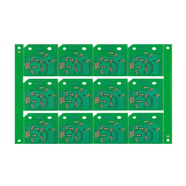
Immersion silver PCB's are flat and usually value less than ENIG but have more dealing with, packaging and storage necessities leading to a shorter shelf life. The problem is that it tarnishes quickly and is adversely affected by touch - very often the silver end changes over time and could be seen as having a rainbow effect. As long as the producers guidelines are followed then silver PCB's are a price efficient answer but there are the extra high quality concerns that should be thought-about. Don't hesitate to contact us if any questions about OSP surface ending PCB. Here is the OSP PCB structure which can help you understand extra about OSP floor ending.
uses a water-primarily based organic compound that rust (oxidation or vulcanization, and so forth.) in normal environment. Another contribution that gold has made for know-how is in the aerospace trade.
Additionally the registration between the layers should be very accurate to make sure that any holes line up. 'What Ever Happened to Molded 3D Circuit Boards?' Plastics World, February 1993, pp. 32-36.
With the long life expectancy and reliability of gold connections and PCBs built-in into spacecraft and satellites, gold is the pure selection for crucial components. The PCB manufacturing course of is an essential factor of the electronics manufacturing lifecycle. PCB manufacturing employs many new areas of know-how and this has enabled important improvements to be made both within the discount of sizes of parts and tracks used, and in the reliability of the boards. The boards are made by using a lot thinner particular person boards, one for each layer, and these are then bonded together to provide the overall PCB. As the variety of layers increases, so the person boards should turn into thinner to prevent the completed PCB from changing into too thick.
Custom message