Latest products
Organic Surface Preservative
by:A-TECH
2020-09-11
This can be carried out with solder paste and reflow or throughout wave soldering. OSP is a process for surface therapy of PCB copper foil primarily based on RoHS instructions, which get rusty in a normal setting with a water-based mostly organic compound. But it needs to simply take away the protecting movie by the flux, so that the exposed clear copper surface can be connected with the molten solder spot in a very brief time.
In this example, OSP is a positive finish if the product being built doesn't require Pb-free wave soldering for thick boards, excessive yield ICT just isn't required, and wire bonding to the surface finish just isn't required. It's best considered a an almost invisible protecting lacquer on the surface of the board.
Each finish comes with its own commerce-offs that you simply’ll should weigh. Which surface end you select will in the end come right down to the design of the PCB, the assembly of its components, and it’s end utility/surroundings.
After a lot considerationMacdermid'sM-Coat OSP is at present our default and favourite leadfree end. OSP is projected for use on 558 million sq ft of circuit boards in 2008 second fiddle toHASL at 737 million sq ft. The major drawbacks are related to solderability, shelf life, re-use of misprinted boards, and multiple heating cycles.
This end requires immersing circuit boards into a tin/lead alloy then eradicating the surplus solder by blowing hot air to it. Nickel acts as a barrier to copper and a floor for SMT placement and a thin layer of gold protects the nickel from oxidation.
If the PCB handed 6 months after manufacturing, then it ought to be baked earlier than SMT. This is the predominant method that has been dominating for a long time.
Another attainable solution may be to use OSP with water soluble flux and perform cleansing prior to ICT (nevertheless each these solutions do add some price). The most important advantage of HASL is superb solderability which is helpful when one wants to achieve complete gap-fill on a fancy double sided PCB. The diagram shown in Figure 3 illustrates how OSP suits with the necessary product attributes.
After two sided reflow the hold time is much more important on an excellent OSP when wave or selective is used. For example, the application may require a end that is low cost, high quantity, corrosion resistant with good ICT properties. One solution might be to make use of ImAg but design the board to mitigate the risk of corrosion by filling the vias with solder mask and shifting any uncovered silver areas far apart.
In addition, its the surface of the copper prior to coating & the coating process. Then its the soldering temperature, time at elevated temperature and the way shortly the cooling is carried out. Then it's also impacted by both air or nitrogen reflow and the levels of nitrogen.
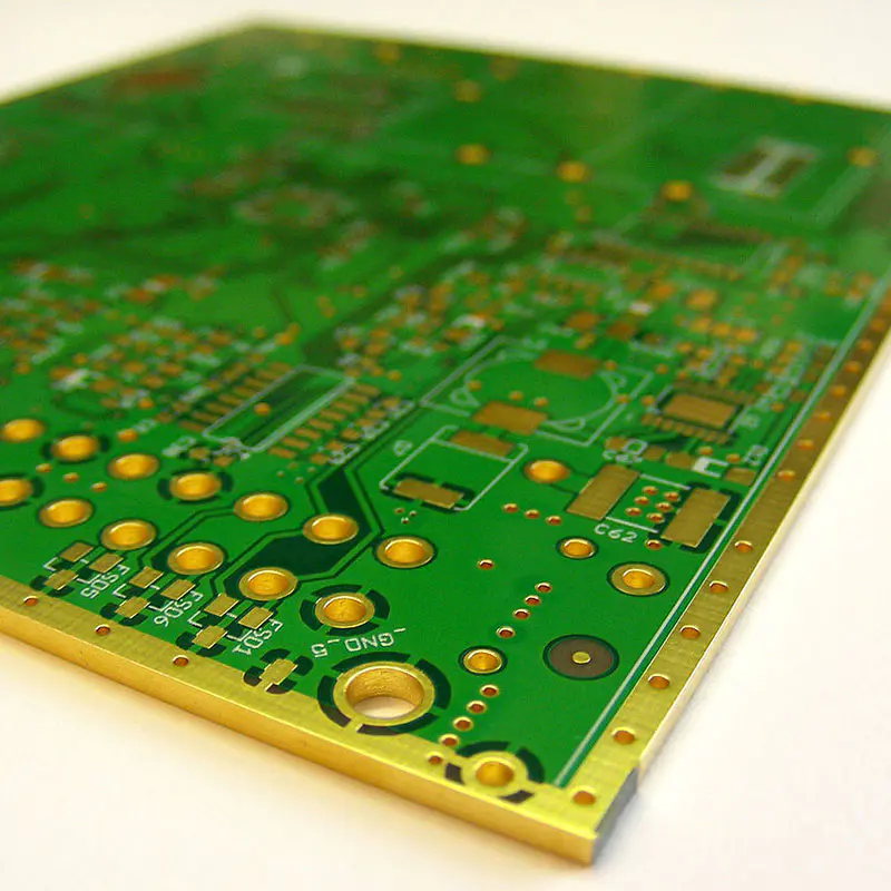
In reality the surface of the board is treated with an acidic cleaner followed by apersulphate microetch to render to wash and improve the floor area, at which point it is then given it's organic coating. The process is selective whereby a reaction take place with the copper on the PCB to form the coating, only a very minimal amount is deposited onto the base laminate.
Custom message