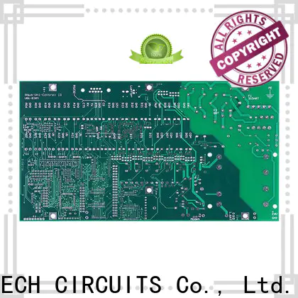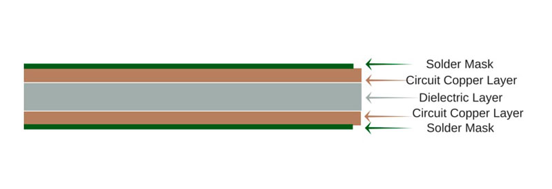
Double sided PCB have two copper layers that can be connected by a copper plated hole, solder mask and idents can also be added on both of top and bottom side, it’s the most popular type of printed circuit boards in industry and it has the highest proportion of demands in the worldwide market.
Double sided printed circuit boards can be used for both through hole and surface mount components, the components can be assembled on both of top and bottom side, so you don’t need to worry about where to put components on the circuit boards, and not need to use through hole components which is usually expensive than SMD one. They’re widely used in different applications, such as power supplies, industrial controls, automotive, LED lighting and many more.

The benefit of double sided PCB
● Increased circuit density
● More flexibility for designers
● Relatively lower costs
● Reduced board size(which can reduce costs)
● Intermediate level of circuit complexity
A-TECH started manufacturing double sided PCB since 2003 and there is 15 years’ experience so far, it’s one of our core business with high fabrication proportion. We’re able to offer 24 hours quick turn service for prototype PCB of double sided and 2 ~ 5 days fast lead time for small to medium volume order, moreover, the longest board size for 2 layers PCB we can fabricate reach 1.5 meters.
| General Specification for double sided PCB in A-TECH | |
| Layer Count | 2 Layer |
| Material Available | CEM3, FR4, High Tg FR4, AL base, PI, Teflon, Taconic, Arlon, Rogers. |
| Max board size | 510*1500mm |
| Board thickness | 0.4-3.2mm |
| Finished copper thickness | 1-6oz |
| Min trace width/spacing | 4/4mil |
| Min hole size | 0.2mm |
| Colour of Solder Mask | Green, Blue, White, Black, Yellow, Red. |
| Colour of Silkscreen | White, Black, Yellow. |
| Surface treatment | HASL, HAL(Lead free), OSP, Gold Plating, Immersion Gold/Tin/Silver, Carbon, Peelable Mask. |
Copyright © 2025 A-TECH CIRCUITS Co., Ltd. | All Rights Reserved
Hello, please leave your name and email here before chat online so that we won't miss your message and contact you smoothly.