Method of checking the electrical function of PCB
by:A-TECH
2021-03-22
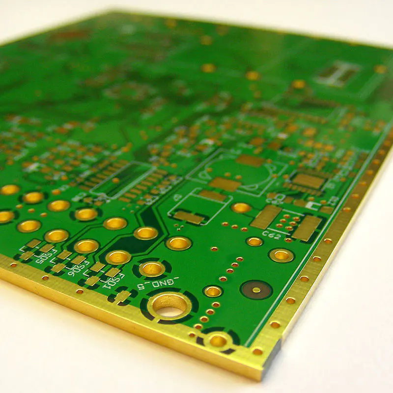
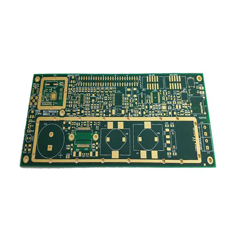
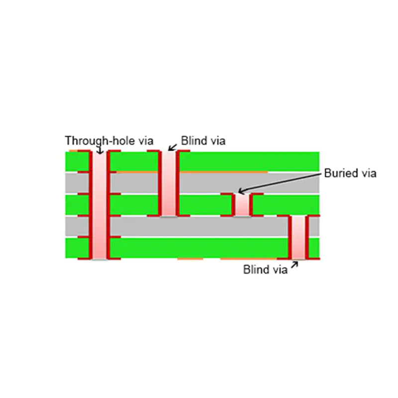
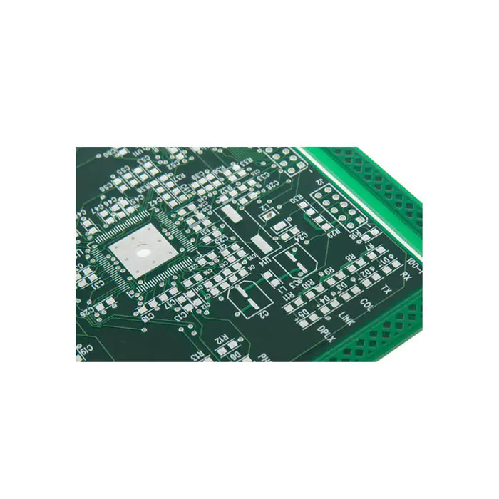
When it comes to PCB electrical function inspection, the first thing that comes to mind is flying probe test. Flying probe test is one of the many methods to check the electrical function of PCB. It is a system for testing PCB in the manufacturing environment. Here we have made a detailed explanation of the main skills and steps in the flying probe test operation, which can provide you with reference and comparison. Flying probe test production steps: First. Import the layer file, check, register, etc., then the two outer lines, change the name fronrear, the internal change ily02 name, ily03, ily04neg (if it is negative), rear, rearmneg. Next. Increase to three, drill two solder resist layers respectively to add three copies, and change the name of fronmneg, rearmneg, and blind buried vias of mehole. Third, copy the two changes of the past fronmneg and rearmneg's D-Code in the 8th round of MIL. We call the front layer of the fronmneg test point, called the rearmneg test point. Fourth, delete the NDK control line hole into a hole, the definition of the hole is unexpectedly discovered. Fifth, the front edge mehole, as a reference layer, the layer fronmneg changes, please check whether the test point is the window of the first layer line. Move the measuring point of the ring test weld to a hole greater than 100mil. The BGA that is sent is immediately measured near the point. Remove the appropriate number of redundant intermediate checkpoints. The same process is the back layer. Sixth, the front edge layer organization is a good test point, fronmneg duplicates, and rearmneg rear layer is duplicated. Seventh: All levels are enabled, and the height is 10.10 mm. Eighth: The leading edge outputs the name of the Gerber file, ily02, ily03, ily04neg, ilyo5neg, rear, fronmneg, mehole rearmneg, met01-02-09 met02, met09 met10. Then Ediapv software first, all the leaders, such as Gerber file front edge, ily02, ily03, ily04neg, ilyo5neg, rear, fronmneg, mehole rearmneg, met01-02-09 met02, met09 met10 layer. Second: Generate a network. Net annotations are key works of art. third. To generate the test file for the test program, make the button, enter the unexpected hole in the D-Code. Fourth: Save. Fifth, the reference point setting is completed. Then test flying machines for them. Of course, we can also use the following keywords to detect: 1. Alignment manual alignment. Strictly speaking, the hole is not in the center of the pad, so when alignment, should the point be placed in the center of the pad as much as possible, or Try to overlap the real hole as much as possible? Generally, if most of the points to be tested are holes, choose the latter. If most of the points are ICs, especially when false open circuits are prone to occur at the IC, the alignment hole needs to be placed in the middle of the pad. 2. Fixed frame The fixed frame is the fixed test bracket, the information with the frame is represented by two boxes, and the outer box is the frame. For such a board, you can directly use the size given by the machine. The information of the frame is represented by a box. We can use the show board command (used when looking at the direction of the board) to see which of the tested pads is on the farthest side. Compare it with the actual board and see it. What is the distance between the board edges. 3. Crossing For the patch panel, the selected single can be tested. We can use this function to test the patch panel whose distance from the pad to the board edge is too small to test. The pallet blocks the untested singles and crosses them out. After the test, put the pallets on the tested single fixed board and select the board that was not tested last time, so that the entire board can be tested through 2 tests. Therefore, we should use the functions provided by the equipment flexibly to fulfill some special needs.
Custom message