Introduction About Pcb Surface Treatment Of Osp
by:A-TECH
2020-09-12
Protection of the surfaces towards further oxidation is relatively easy, through the use of vacuum or inert environment. Removal of the native oxide layer is more troublesome; physical or chemical cleansing methods have to be employed and the surfaces can be protected by e.g. gold plating.
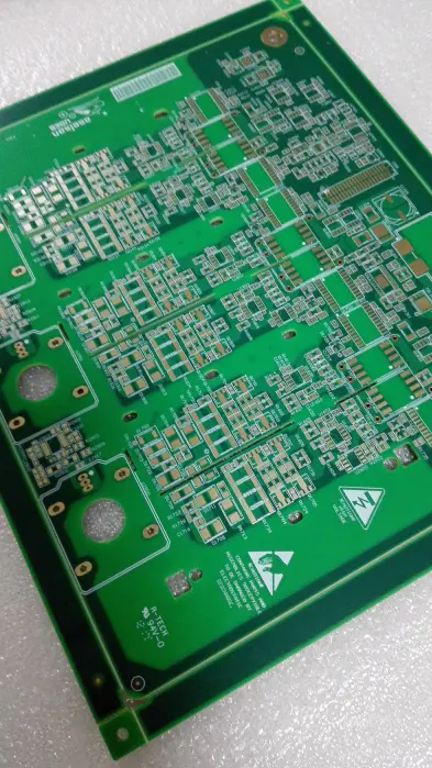
When in comparison with the other high four finishes, ENIG, Lead Free-HASL, immersion silver and OSP, ENEPIG outperforms all on the after-meeting corrosion stage. OSP (Organic Solderability Preservative) or anti-tarnish preserves the copper surface from oxidation by applying a very thin protective layer of material over the exposed copper often utilizing a conveyorized process.
The gold layer must be sufficiently thick and non-porous to offer protection for cheap storage time. Thick gold metallization additionally limits selection of soldering alloys, as tin-based solders dissolve gold and kind brittle intermetallics, embrittling the joint. Thicker gold coatings are usually limited to use with indium-primarily based solders and solders with excessive gold content material. Stainless metal is materials which is troublesome to solder due to its stable, self-healing surface oxide layer and its low thermal conductivity. A solution of zinc chloride in hydrochloric acid is a standard flux for stainless steels; it has nonetheless to be totally eliminated afterwards as it might trigger pitting corrosion.
If in case of any harm, it’s very straightforward to verify and replace the particular failure elements. The digital components and their polarities on a properly designed, printed circuit boards are clearly labeled on the board. The printed circuit boards are very important part of a modern electronic gear. A basic PCB circuit consists of a very large variety of passive and lively components.
All the parts are linked from side to side with traces on the board. It is absolutely attainable to develop very large circuits on small printed circuit boards with the availability of very small sized digital elements. These are just a few examples of how printed circuit boards can be utilized in industries and sectors, however the potentialities are endless. If your small business requires PCB manufacturing and assembly, then please get in touch with us.
The Printed Circuit Board (PCB) is essential in all electronic gadgets, which are used either for home use, or for industrial function. Apart from electrically connecting, it also gives mechanical support to the electrical elements.
Manual layouts are created with the assistance of CAD drafting, and the automated router helps within the creation of the designs routinely. The designers normally choose the handbook means of designs, since they can implement their very own ideas and methods in them. A PCB populated with electronic components known as a printed circuit assembly (PCA), printed circuit board meeting or PCB Assembly (PCBA). In casual use the term “PCB” is used each for naked and assembled boards, the context clarifying the that means.
Custom message