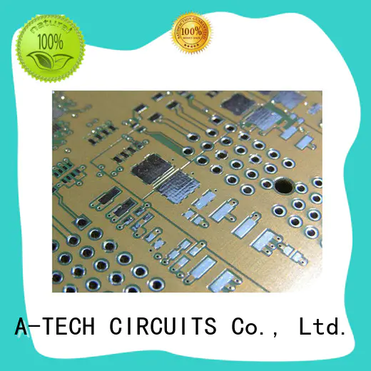
Company Advantages1. The production of A-TECH enig pcb finish is resource-efficient and causes less pollution to the environment.
2. The product is durable in use. It has been tested with guaranteed service life and its structure is strong enough to withstand years of uses.
3. This product is not easy to get deformed. It has passed the dimension stability testing, which proves that it is able to retain its original shape.
4. A-TECH CIRCUITS Co., Ltd. has highly qualified agents responsible for product sales and providing quality global customer service.
5. All employees in A-TECH CIRCUITS Co., Ltd. will integrate culture into their work and ensure the company's continued success.
HAL(Lead Free), the full name is Hot Air leveling with Lead Free. Compared with HASL, the main difference for HAL(Lead Free) is the element of material which do not contain Lead(Pb), so it’s RoHS Compliant and it’s much more popular and widely used in PCB manufacturing.
HAL(Lead Free) requires higher run temperatures for lead free solder and longer contact time, the production cost for HAL(Lead Free) is slightly higher than HASL(Tin/Lead).
The manufacturing process of HAL(Lead Free) is similar to HASL(Tin/Lead), the circuit boards will be submersed in molten solder(Lead Free). This solder will cover all the exposed copper surfaces. Upon retraction from the solder, high pressure hot air is blown over the surface through air knives, this levels the solder deposit and removes the excess solder from the surface of printed circuit boards.
The typical thickness of HAL(Lead Free) is 1-40um and the shelf life is 12 months.
The advantages of HAL(Lead Free) surface finish
● Good solderability / wettability
● RoHS Compliant
● Good reflow properties
● Large processing window is allowed
● Multiple thermal excursions
● Can be widely used
The disadvantages of HAL(Lead Free) surface finish
● Uneven surface
● Not suitable for PCBs with fine pitch
● Thermal shock
● Solder bridge
● Plugged or Reduced plated through holes
A-TECH have HAL(Lead Free) surface finish in house, It’s basically the highest proportion of finish used for circuit boards without fine pitch or high density layout. We don’t have any additional cost for HAL(Lead Free) surface finish.
Company Features1. As a company growing steadily in recent years, A-TECH CIRCUITS Co., Ltd. has gained market recognition for excellence in manufacturing enig pcb finish .
2. The
osp pcb finish technology also contributes to the wide application of osp pcb .
3. We strive for a culture of integrity in our people, partners, and suppliers. To this end, we have established a dedicated ethics and compliance program to ensure that ethical and compliant behavior is deeply embedded throughout the company. Ask online! Except for improving the economic benefits to society, the company is striving to create a healthy and fair market. We regard it as our own responsibility to promote the market to grow healthily in terms of monopolies, fair trade, and profitability. Ask online! We take steps to formalize our environmental practices through the development of environmental policy. This will involve understanding and recording key environmental impacts, investigating opportunities for reducing these impacts. We have adopted the policies for sustainable resource utilization. We enhance the environmental management system constantly by determining, realizing and revising environmental goals periodically in order to meet the requirements of our environmental awareness.


