loading

A-TECH  >  AI - Page Sitemap  >  highly-rated enig pcb finish solder Supply at discount
highly-rated enig pcb finish solder Supply at discount

highly-rated enig pcb finish solder Supply at discount
  • highly-rated enig pcb finish solder Supply at discount

highly-rated enig pcb finish solder Supply at discount

The production of A-TECH enig pcb finish follows the strict production process. Its working panel is coated with a photo-sensitive epoxy-based ink, which can ensure its insulation resistance
Inquire Online
Get the latest price
Quantity Needed:
Pieces
E-mail:


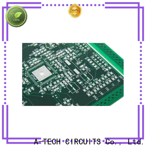
HASL, the full name is Hot Air Solder Leveling, it’s one of the traditional surface finish on printed circuit boards with long successful history.

To make the HASL finish, the circuit boards will be submersed in molten solder(Tin/Lead). This solder will cover all the exposed copper surfaces. Upon retraction from the solder, high pressure hot air is blown over the surface through air knives, this levels the solder deposit and removes the excess solder from the surface of printed circuit boards.

HASL (Tin/Lead) surface finish is not RoHS Compliant, so it can be only available where RoHS exemption is permitted. The typical thickness of HASL is 1-40um, and the shelf life can reach to 12 months.


The advantages of HASL surface finish

● Excellent solderability / wettability
● Good reflow properties
● Low cost in manufacturing
● Large processing window is allowed
● Multiple thermal excursions
● Can be widely used


The disadvantages of HASL surface finish

● Uneven surface
● Not suitable for PCBs with fine pitch
● Thermal shock
● Not RoHS Compliant
● Solder bridge
● Plugged or Reduced plated through holes


A-TECH have HASL surface finish in house, it’s mainly used to build single sided or double sided PCBs with high solderability requirements but low manufacturing cost and without RoHS Compliant requirement.


Exclusive use of high quality materials is anticipated in the manufacturing processes of enig pcb finish. These materials are pinpointed through direct experience and selected from among the best and most innovative on the market.
Useful design: enig pcb finish is designed by a group of creative and professional experts based on the findings of their investigation and research of customers' needs. Being laminated by advanced vacuum lamination equipment, it has a uniform dielectric thickness after lamination
A-TECH enig pcb finish presents a perfect marketing effect with its appealing design style. Its design comes out from our designers who have put their efforts on the innovation of design day-and-night. It stands out for its impact endurance performance
The innovative design gives A-TECH enig pcb finish more aesthetic appeal. It is vacuum-sealed, which can greatly reduce the bulk of the overall cargo
Thanks to the team of diligent professionals, A-TECH enig pcb finish is manufactured according to the requirement of lean production. It is lead-free and environmental-friendly and has passed SGS test
A-TECH CIRCUITS Co., Ltd. Standardized production mode is adopted to standardize every step in the production process, so as to achieve the purpose of comprehensively improving the resource utilization rate, reduce the loss of materials in the production process to the greatest extent, optimize the production cost, and thus ensure the [ 10219] On the premise of the same quality and performance, the added value is high and the price is better. Compared with similar products, the cost performance is high, and the purchase of our products can save more costs.
Product Message
Chat Online 编辑模式下无法使用
Chat Online inputting...
Please hold on and we will get back to you soon