Company Advantages1. The surface treatment of A-TECH press fit pins pcb mainly includes degreasing, anodizing, sandblasting, painting, and laser engraving. It has to go through surface inspection to guarantee burr free. It is vacuum-sealed, which can greatly reduce the bulk of the overall cargo
2. The product is widely used in the global market now and is believed to have a wider application in the future. It totally conforms to the UL Flame Rating of 94V-0
3. This product has stable performance and long service life. Its working panel is coated with a photo-sensitive epoxy-based ink, which can ensure its insulation resistance
4. The product has withstood the tests of our professional QC team as well as the authoritative third party. Its robust structure allows it to be used in harsh environments
5. Quality-focused: the product is a result of pursuing high quality. It is strictly inspected under the QC team who has the full right to take charge of the quality of the product. It is widely used in different electronics industries, such as telecommunication and consumer electronics
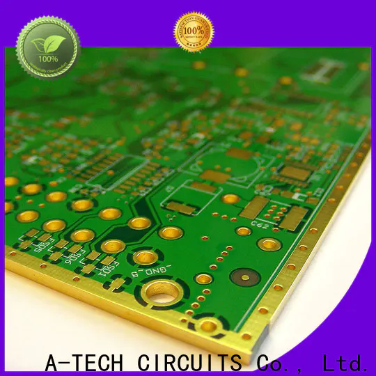
PCB edge plating, also called sideplating, it refers to copper plating that runs from top side to bottom side and runs along at least one of the perimeter edges. Portions of the printed circuit’s contour but also partial areas within the circuit board can be metalized.
In order to make PCB edges metalized, the printed circuit boards must be routed before through hole copper plated process, because the metallization of the PCB edges take place during this copper plating process. The ENIG (Immersion Gold) finish is preferred for PCB edges after copper plated.
PCB edge plating technology is used for several industries, especially in application that require better support function, such as:
● Edge connections and protection
● Edge soldering to improve fabrication
● Better support for connections such as boards that slide into housing connection
● Improving current-carrying capabilities for better EMC performance such as high frequency PCB
A-TECH has lots of manufacturing experience for PCB edge plating, and we’re able to control high quality for edge plating without burrs. Please try to contact our sales experts for any technical details.
Company Features1. A-TECH has been gradually leading via in pad technology industry for its improving service and higher quality annular ring pcb . Integrating finest technology and excellent staff together, A-TECH has been always offering through hole pad with high quality.
2. A-TECH CIRCUITS Co., Ltd. has advanced production line and professional R&D team.
3. The strong technology capability makes A-TECH CIRCUITS Co., Ltd. stands at the forefront of the pcbs definition industry. A-TECH CIRCUITS Co., Ltd. aims to bring the best thick copper pcb with professional service. Ask!
