Electronics Industry
by:A-TECH
2020-04-16
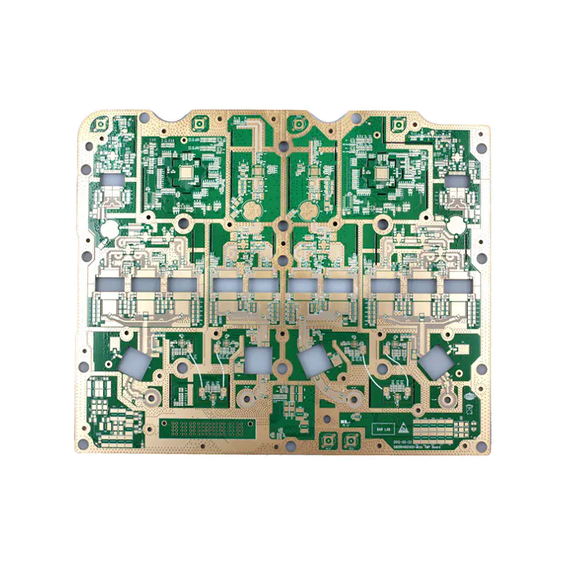
One of the most important links from design completion to processing and manufacturing of electronic products is the processing of PCB circuit boards.
However, most of the bare boards processed by PCB need to be pasted and assembled by chip mounters.
Then the problem is coming, and the current electronic products are developing in the direction of small and portable.
When your design PCB board is especially small, and some electronic product modules are as small as small as a few centimeters square, PCB processing and manufacturing is easy to say, but when it comes to PCB Assembly, such a small area is put on the Mounter for assembly, which brings problems. There is no way to assemble the production line!
Here, it is necessary to make a small piece of PCB into a suitable area that meets the requirements of the assembly machine, or to make a yin and yang board, which is more convenient for patch assembly.
In general, the manufacturer of the board will provide the service of the puzzle, but in the design of the Altium Designer software design, in addition to more clearly showing the Designer's intentions, there are many benefits.
The benefits are as follows: you can associate the jigsaw puzzle file with the source board according to your desired direction, and the changes of the source board will be automatically updated to the jigsaw puzzle. You can put several different boards together to spell Yin and Yang boards (Alternating front and back)
How to assemble in Altium Designer?
Here we use an example to introduce the process and Operation steps of splicing in Altium Designer. 1. First determine the size of the board.
This can be seen with Report> Board information.
As shown in the following figure, this board is used as an example PCB board with a size of 75. 18x30. 23mm.
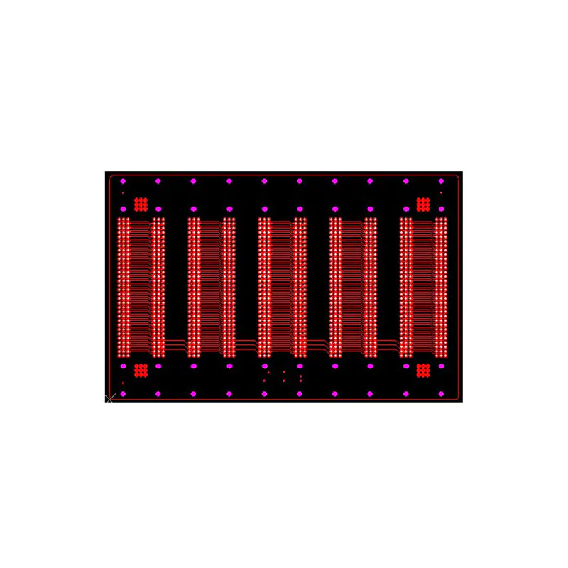
We will spell out a 2x 2 PCB array in a new PCB diagram.
2. Use File> New> PCB to create a rectangular PCB with a size of 160 x, 2 layers of signal layer, no power layer and through hole.
The newly created PCB for splicing is as follows, save.
3. On the newly created PCB, Click Place> Embedded Board Array/Panelize. As shown in.
This is our imposition function. Click in and see the following figure to output the length and width (This parameter is generally slightly larger than the original board. Depending on your needs).
Select the PCB Document you want to spell in the PCB Document column.
Then, enter the number of horizontal and vertical rows to be spliced in the Row and Column element input boxes of Column Count and Row Count. Here, choose 2.
4. After setting the above parameters, click OK to place the array board on the PCB diagram. Adjust the position just in the middle.
And reposition the origin of the PCB to the origin of the array board.
5. Enter the Layer color manager below and rename Mechanical2 to Route Cutter Tool Layer. The lines drawn on this Layer are defined as the traces of milling Cutter milling through PCB;
The Mechanical5 is renamed FabNotes, and the line drawn on this layer is defined as the V slot to be washed out on the PCB (V-GROOVE)The routing.
The following figure shows the array board that draws the details.
Note that we need to draw the Route Cutter Tool Layer routing and FabNotes routing on the PCB array board, during these routing, we should let the CAM drawing processing personnel of the processing board factory understand our specific needs and intentions.
However, the specific Cut or V slot is subject to our communication and exchange with the engineers of the board factory. This is just a schematic diagram.
Finally, the PCB array board is converted into Gerber and other processing drawing files.
Give it to the PCB processing board factory and communicate the specific process requirements and details with the board factory.
The jigsaw puzzle is updated synchronously with the source PCB. If any changes are made on the source PCB, these changes are updated with one click in the PCB jigsaw puzzle file.
Place a pad in the source PCB as shown below.
Then in the PCB puzzle file, click Refresh to Refresh, and each of these boards will have such a pad. Update synchronously with the source board. As shown below. How to put different PCB together?
To put different PCBs together, you only need to select a PCB File and spell out the array.
Then select other PCB files and spell out the array. As shown in.
It should be noted here that for different PCB piecing together, the layer setting and board thickness setting of those PCB that need to be pieced together need to be completely consistent. Can be put together for processing.
If you want to spell Yin and Yang boards, the method is to use this jigsaw puzzle function to place a board array first, and then select the mirror when placing another board array.
Similarly, the yin and yang plates must have the same thickness for each layer. Can be put together for processing.
Custom message