Latest products
Circuit board processing and the difference between the positive and negative
by:A-TECH
2020-05-15
Vacuum laminating machine, reduce the pressure to reduce flow glue, try to keep more amount of resin, as resin affect epsilon r, resin to save more, epsilon r will be lower.
Control layer thickness tolerance.
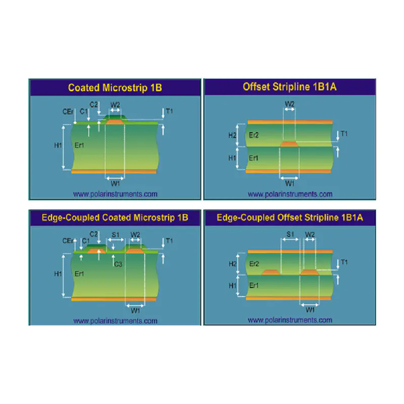
Because the PCB circuit board thickness is not uniform, suggests that the medium thickness change, affects Z0.
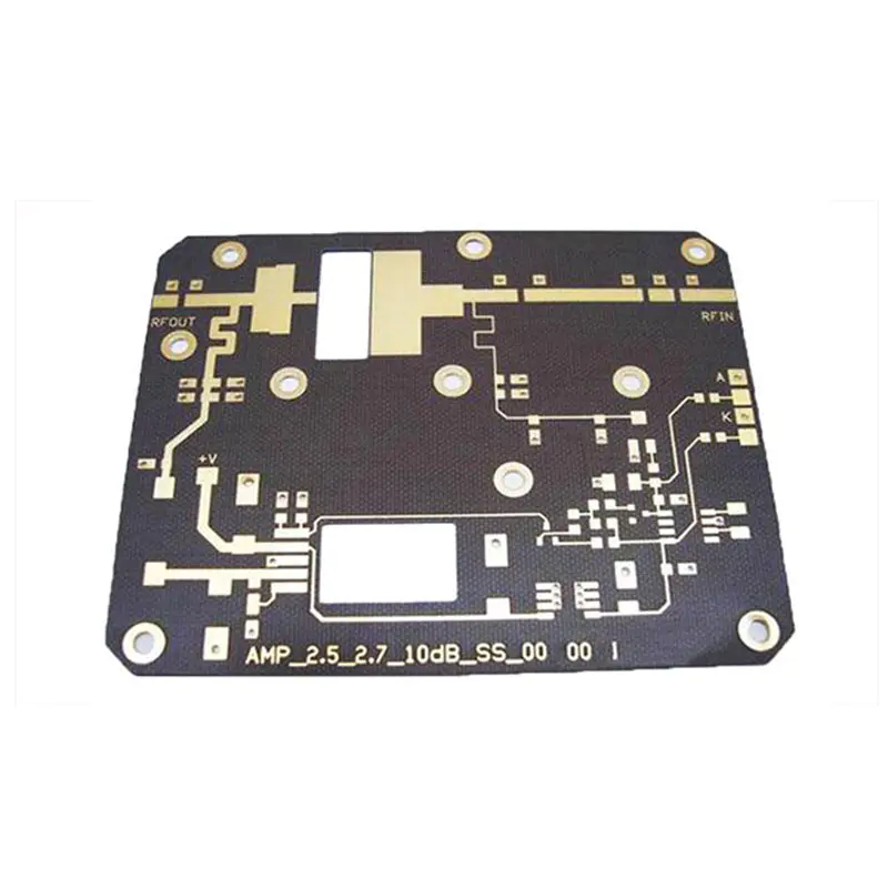
Strictly according to customer requirements of the PCB circuit board plate model under the expected, the model of fault, epsilon r wrong, thickness, PCB manufacturing process to completely, also destroyed.
Because Z0 affected by epsilon r, finished products profes sional avoid absorbing water, because water epsilon r = 75, of Z0 can make a big decline and the instability of the effect.
PCB PCB board face resistance welding can reduce Z0 value of the signal lines 1 ~ 3 Ω, theoretically resistance welding thickness shoulds not be too thick, in fact is not significantly affected.
Copper wire surface contact with the air (
εr = 1)
, so the measured Z0 value is higher.
But in resistance measurement Z0 will decline after welding Ω 1 ~ 3, the reason was that the resistance welding epsilon r of 4.
0, much higher than air.
Lining board must find out the wire gap, protruding mouth, to 2 GHZ high-speed signal, even zero.
5 mm gap, also must be discarded;
Control the inner line width, and defects is the key.
Circuit board processing of negative: usually we speak tenting process, the use of acid etching solution for negative film because the film production, to the line or copper surface is transparent, and not part of it is black, after line process exposure, transparent part because of dry film resistance agent light chemistry hardening, the next development process will not wash it hardened dry film, so just bite in the etching process dry membrane rinse away part of the copper foil (
Black film part)
Wash it, and keep dry film is not belong to us to line (
The part of transparent film)
Circuit board feature: usually we speak of the pattern, its use for the alkaline etching solution if positive to negative, to the line or copper surface is black, and not part of it is transparent, in the same way after line process exposure, transparent part because of dry film resistance agent light chemistry hardening, the next development process will take no hardened dry film hedge, followed by lead tin plating process, the tin lead plating in the previous process (
Development)
Dry film hedge copper surface, and then to membrane action (
Remove hardened dry film) due to light
, and in the next process etching with alkaline liquid bite off without the protection of a tin lead copper foil (
The part of transparent film)
, the other is the line (
Black film part)
Custom message