Company Advantages1. The production of A-TECH press fit pins pcb is adjusted to meet the needs of customers. It is lead-free and environmental-friendly and has passed SGS test
2. This product not only acts as a functional and useful element in a room but also a beautiful element that can add to the overall room design. It has increased power densities which guarantee its long service life
3. The product features strong corrosion resistance. Both the metal parts and mating faces are made of anti-corrosion materials such as stainless steel, plated steel, carbon, or ceramic. Being laminated by advanced vacuum lamination equipment, it has a uniform dielectric thickness after lamination
4. The product is of flexibility. Unlike some batteries which need to be placed in the upright position, it can operate in any position and offer good impact tolerance. A smooth part is added on its PTH line to reduce the roughness of through hole
5. It offers a high level of structural stability. It spans multiple floors and can deal with factors like thermal expansion and contraction, water diversion and building sway and movement effectively. Thanks to the up-to-date vacuum DES line, it is manufactured with fine traces and high density
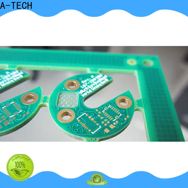
Depth control routing(milling) is also known as Z-axis milling or level milling, it refers to partial routing in printed circuit board manufacturing with a variable level elevation at the PCB edge or within PCB.
Control depth routing technology supports a high end market with the need for accuracy, miniaturization, process stability and the need for productivity, and depth routing option allows for very complex designs, bended boards and structures to be processed with fine precision.
Depth control routing technology have great advantages in PCB assembly as the special shape of depth routing.
● It can avoid cold soldering as siphonic effect use NPTH step stair slot
● Use the step stair in middle of PCB apply in special module application, and degrade the height of PCB assembly, achieve refinement and miniaturization
● Use the step stair of PCB edge make card slot is favor for PCB fixed and installation
● Use Special size NPTH step stair as resonant cavity of microwave signal, degrade signal loss and other special function.
A-TECH has manufacturing capability to build various types of depth routing with different size and depth, no matter on the PCB edge or within the PCB, and the precision tolerance can be controlled as +/-0.1mm(4mil).
Company Features1. Under advanced equipment and proven technology, A-TECH CIRCUITS Co., Ltd. has become an advanced manufacturer of pcb edge plating process .
2. Based on years of market expansion experience, we have become a global market player in this industry, especially in the markets of North America, Asia, and the Middle East.
3. A-TECH CIRCUITS Co., Ltd. has been encouraged to provide better service for customers. Contact!

