CAD and CAM operations in PCB design
by:A-TECH
2021-03-09
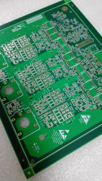
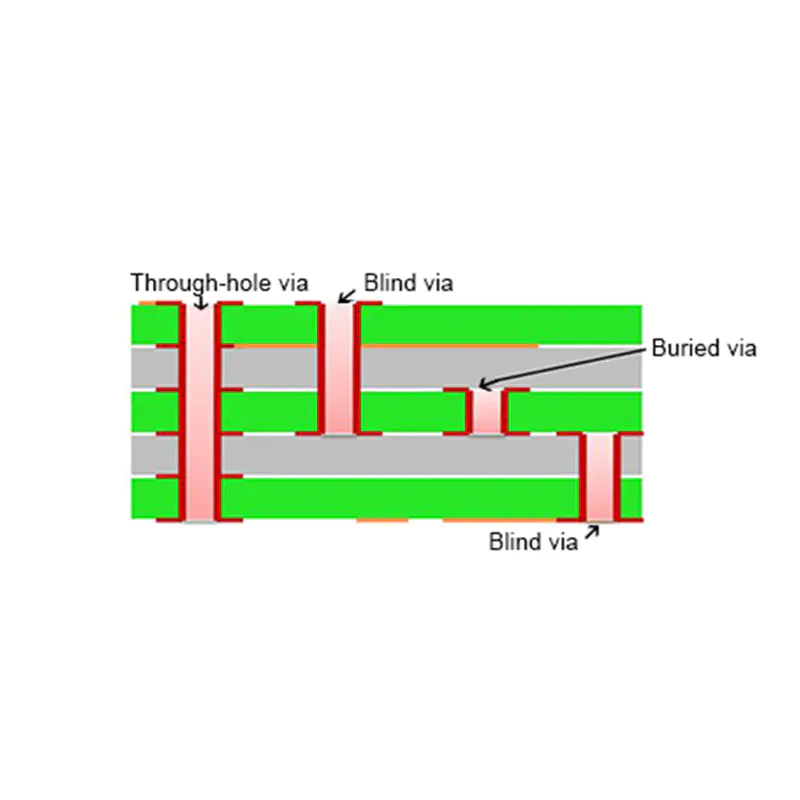
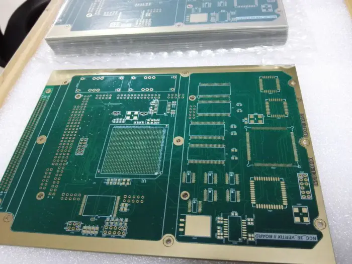
About CAD and CAM operations will be introduced below. A. Enter Gerber Data into the used CAM system, at this time apertures and shapes must be defined. Currently, there are many PCB CAM systems that can accept the IPC-350 format. Some CAM systems can generate external NC Routing files, but general PCB Layout design software does not generate this file. Some professional software or independent or with NC Router can set parameters and directly output the program. Shapes are round, square, rectangular, and also have more complex shapes, such as the thermal pad in the inner layer. When starting to design, the relationship between Aperture code and shapes must be clearly defined, otherwise the subsequent series of designs cannot be carried out. B. Check list during design After reviewing based on the check list, the possible yield rate and cost estimate of the production material number can be known. C. Working Panel layout precautions: - PCB Layout engineers will make some auxiliary marks for reference in order to help remind or pay attention to certain matters when designing, so they must be removed before entering the layout. The following table lists several items and their impact. -The size of the layout will affect the profit margin of the item number. Because the substrate is the main raw material cost (optimization of layout can reduce sheet waste); and proper layout can increase productivity and reduce defect rates. Some factories think that fixing certain working dimensions can meet the maximum productivity, but the cost of raw materials increases a lot. The following are some considerations: general production costs, direct and indirect raw materials account for about 30-60% of the total cost, including substrates and films , Copper foil, solder mask, dry film, drill bits, heavy metals (copper, tin, lead, gold), chemical consumables, etc. The consumption of these raw materials is directly related to whether the layout size is appropriate. When most electronic factories do circuit layout, they will do contiguous design to maximize productivity during assembly. Therefore, the designer before the PCB factory should communicate closely with the customer so that the size of the contiguous Layout can have the best utilization when the layout is made into a working panel. To calculate the most appropriate typesetting, the following factors must be considered. 1. The minimum number of knives and the maximum utilization rate of substrate cutting (cutting method and edging treatment must be taken into account). 2. The use size of copper foil, film and dry film must match the size of the working panel well to avoid waste. 3. When connecting pieces, the minimum size between pieces, and the minimum size of the board edge reserved for tools or alignment systems. 4. The possible maximum size limit or effective work area size of each process. 5. Different product structures have different production processes and different layout restrictions. For example, for gold finger boards, the layout spacing must be larger and have directional considerations. The test fixture or test sequence regulations are also different. Larger working size can meet greater productivity, but the cost of raw materials will increase a lot, and equipment manufacturing capabilities need to be improved. How to achieve a balance point, design criteria and the experience of engineers are very important. -In the process of layout of working Panel, the following matters must be considered to make the process smooth, and the matters needing attention in layout are shown.
Custom message