Analysis on the practical skills of pcb board wiring
by:A-TECH
2021-03-22
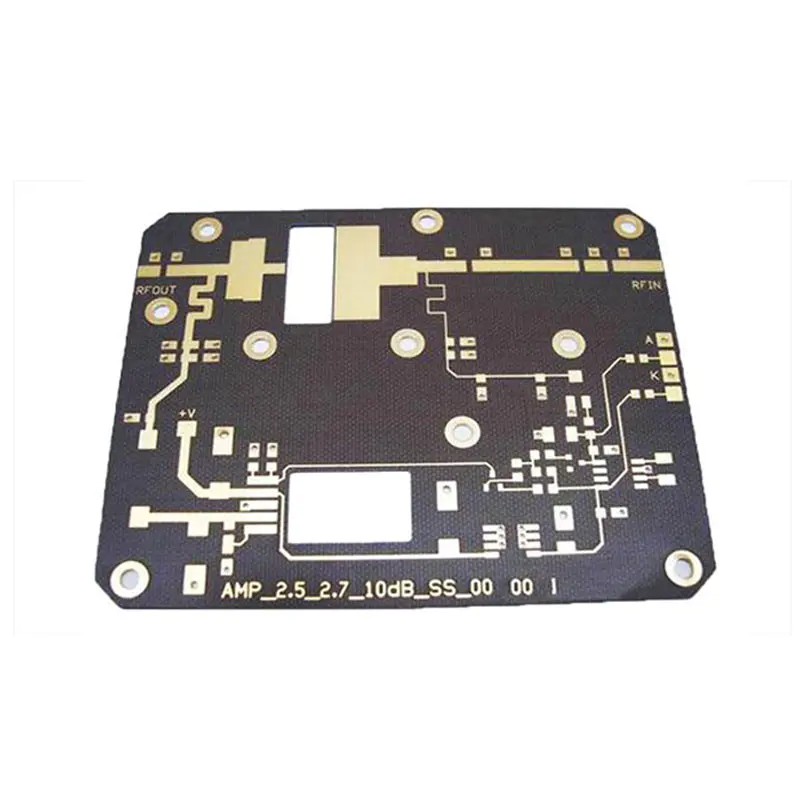
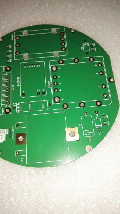
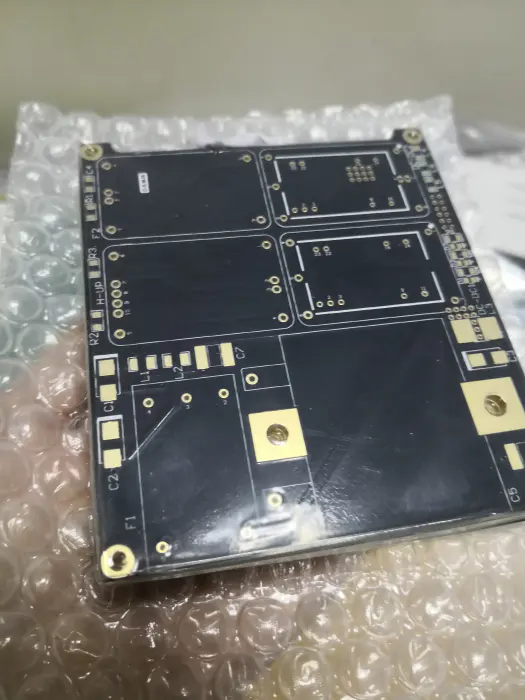
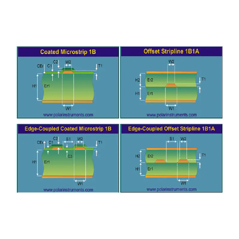
When it comes to PCB board wiring, I have to mention the design of the circuit board. First determine the size of the board in the circuit board design. The large size of the PCB will cause the printed line to be longer, the impedance will increase, the anti-drying ability will decrease, and the cost will increase. If it is too small, the heat dissipation is extremely poor, and adjacent lines are easily disturbed. After determining the size of the PCB, determine the swing position of the special component. Finally, according to the functional units, layout all the components of the circuit. Regarding the layout, one principle is to separate digital and analog as much as possible, and one principle is that low-speed should not be close to high-speed. The most basic principle is to separate digital grounding from analog grounding. Since digital grounding is a switching device, the current is large at the moment of switching and small when it is not moving. Therefore, digital grounding cannot be mixed with analog grounding. A recommended layout can be as shown in the figure below. The wiring of the circuit board is best to adopt a full straight line according to the flow of the signal, and it can be completed with a 45° broken line or a circular arc curve when turning is required, so as to reduce the external emission and mutual coupling of high-frequency signals. The wiring of high-frequency signal lines should be as short as possible. According to the operating frequency of the circuit, the length of the signal wiring should be selected reasonably, which can reduce the distribution parameters and reduce the loss of the signal. When making a double-sided board, the wiring on two adjacent levels is best to be perpendicular, oblique or curved to intersect each other. Avoid mutual parallelism, which can reduce mutual interference and parasitic coupling. Before automatic wiring, interactively route the wires with higher requirements in advance. The edges of the input end and the output end should not be adjacent and parallel to avoid reflection interference. When necessary, you can add a ground wire for isolation, and the wiring of two adjacent layers should be perpendicular to each other, because parallel is easier to produce parasitic coupling. The distribution rate of automatic routing depends on a good layout, and the routing rules can be preset, such as the number of wire bends, the number of vias, and the number of steps. Generally, explore the wiring first, quickly connect the short wires, and then use the labyrinth wiring to optimize the global wiring path of the wiring to be laid. It can disconnect the laid wires as needed and try to rewire them to improve The overall wiring effect. PCB has always insisted on using superb technical force, sophisticated production equipment, perfect testing methods, product quality higher than industry standards, and warm and thoughtful service, which has won praise and welcome from global merchants and users. Here to enter the pricing page https://www./QB
Custom message