Analysis on the function and purpose of PCB solder mask
by:A-TECH
2021-03-21
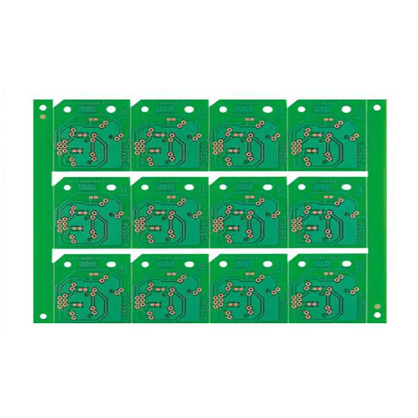
Our common solder masks are spot welding, seam welding, and butt welding. Generally, when we perform the solder mask process, there will be defects such as uneven solder mask, false copper exposure, base material bumps, and broken wires. Pay special attention to the operation points of each step when handling solder mask. In addition, we all know that the solder mask refers to the part of the board to be painted with green oil, but in fact this solder mask uses a negative output, so after the shape of the solder mask is mapped to the board, it is not painted with green paint. Solder mask, on the contrary, exposed the copper skin. Usually in order to increase the thickness of the copper skin, the solder mask is used to scribe lines to remove the green oil. The role of the solder mask in controlling solder defects during the reflow soldering process is important, and the PCB designer should minimize the spacing or air gaps around the pad features. Then why do we do solder mask? I have listed the following points for the purpose of solder mask: 1. Leave the through holes and their pads on the board to be soldered, cover all the lines and copper surfaces, prevent short circuits caused by wave soldering, and save soldering tin Dosage. 2. Prevent moisture and various electrolytes from oxidizing the circuit and endanger the electrical performance, and prevent external mechanical damage to maintain good insulation on the board. 3. As the board becomes thinner and the line width becomes thinner and thinner, the insulation problem between the conductors is highlighted, and the importance of the insulation performance of the solder resist is also increased. For the solder mask process, I don't think there will be too many changes, but process innovation is everywhere, and future development will encounter various challenges, and challenges are everywhere. Material, equipment, and PCB manufacturers will face challenges and even great pressure to survive. Domestic PCB manufacturers are at a relative disadvantage in HDI, automotive boards, and IC substrates, and need more investment. It requires closer cooperation between material vendors, equipment vendors, and manufacturers rather than pure sales relationships. Of course, different companies need to position their products differently. They should not all develop into HDI, automotive electronics PCB boards, and IC packaging substrates. For companies, it is not the harder the better, nor the more sophisticated, the better. The one that suits you is the best. Ok. High-precision multi-layer pcb manufacturers, with the same quality for more than ten years, use ingenuity to do every circuit board. Single and double-sided proofing, small and medium-sized batches are shipped in 3 days, and once won a good reputation in the industry!
Custom message