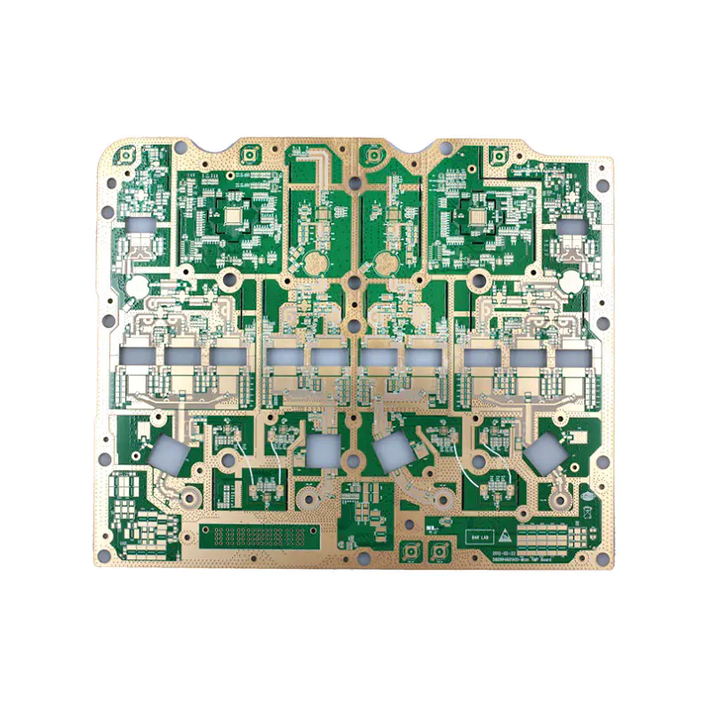
Latest products
Analysis of Cases of Design Mistakes by Shenzhen Jedduobang Clients (2)
by:A-TECH
2021-03-21
16) When forming the gong board, in order to avoid the gong knife injury and the wiring, there is a minimum distance between the wiring and the shape in the design, as shown in the red box in Figure (17). Which of the following descriptions are correct (C, D, E) A) When the gong board is shipped, the distance between the trace and the outline line shall not be less than 0.1mm, if it is a V-cut panel, the distance between the trace and the V-cut center line shall not be less than 0.4mm. B) The outline of the trace when the gong is shipped The line spacing is not less than 0.2mm, if it is a V-cut panel, the distance between the trace and the V-cut center line cannot be less than 0.4mm. C) When the gong board is shipped, the distance between the trace and the outline line is not less than 0.3mm, if it is a V-cut panel. The distance from the V-cut center line cannot be less than 0.4mm D) When the gong board is shipped, the distance between the trace and the outline line is not less than 0.4mm, if it is a V-cut puzzle board, the distance from the V-cut center line cannot be less than 0.4mm E) The gong board is shipped When the distance between the trace and the outline line is not less than 0.508mm (20mil), if it is a V-cut panel, the distance between the trace and the V-cut center line cannot be less than 0.4mm. Figure (17) 17) The following figure is the trace attribute setting diagram of protel99. The difference between Figure (18) and Figure (19) is that the 'keepout' is ticked. What is the difference between the wiring in the two? (B) A) The effect is the same, and both wiring can be made B) The effect is different on the physical board. The wiring in Figure (18) can be implemented on the physical board, but the wiring in Figure (19) cannot be implemented on the physical board. If the lock cannot be output to Gerber, the trace will be missed on the physical board. 18) The design project adopts a 5mm line-width drawing board shape. May I ask the circuit factory to draw the gongs (gongs: the itinerary diagram of the gongs). The reference point is the gong side, as shown in Figure (20) (B) A) Inner B) Centerline C) Outer D) Either way, it doesn’t matter as long as the gong is inside the line, as shown in Figure (20) 19) as shown in Figure (21) It shows that the place pointed by the arrow is a short circuit caused by copper paving. The file adopts pads design. How did the short circuit cause this place (A) Figure (21) A) After the customer modified the circuit design, the electrical copper paving was not performed again. . The circuit board factory is to restore copper (using Hatch). After the restoration, the arrow in the figure is still the effect before the modification, so the physical board is short-circuited. If the responsibility is divided into the customer B) The circuit board factory should carry out electrical copper plating, which is the responsibility of the factory 20) As shown in Figure (22), the red box is the process side. What is the standard process side ( B) A) minimum 2mm, conventional is 5mm B) minimum 3mm, conventional is 5mm Figure (22) 24) Figure (23) is a screenshot of the circuit, what is the minimum line width and gap accepted (C) A) minimum line width The line gap shall not be less than 4milB) The minimum line width and line gap shall not be less than 5mil C) The minimum line width and line gap shall not be less than 6mil, it is recommended to be greater than 6mi as much as possible to improve the yield rate (23)
Custom message