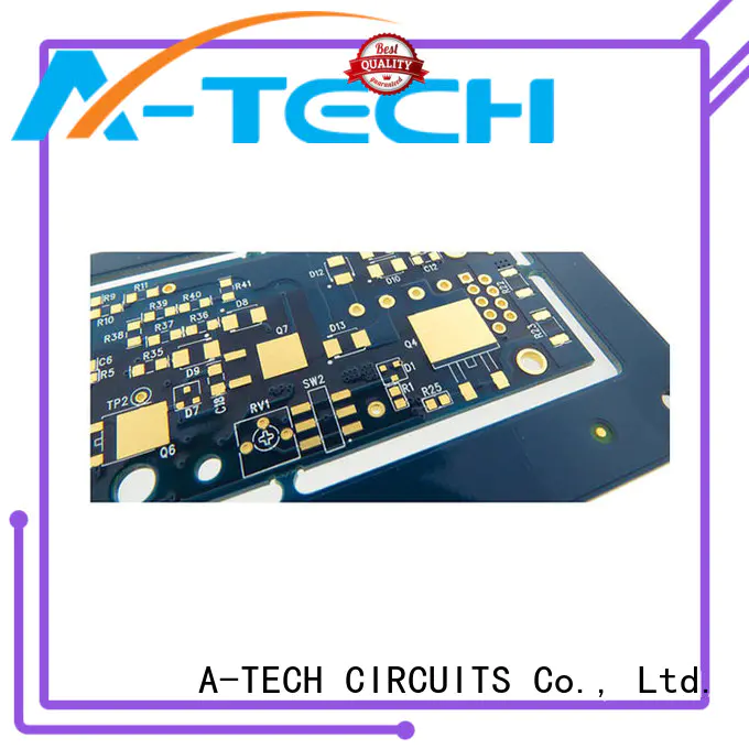
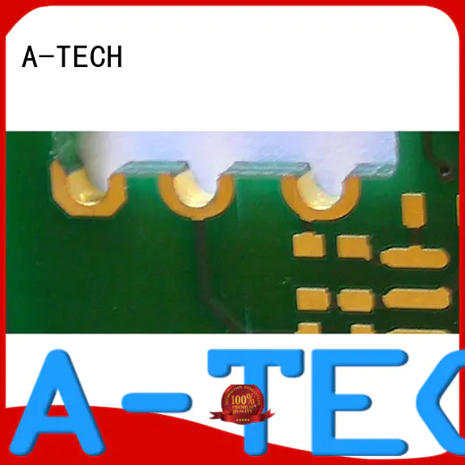
via in pad technology-lead free hasl pcb The designing and developing of via in pad technology-lead free hasl pcb in A-TECH CIRCUITS Co., Ltd. requires stringent testing to ensure quality, performance, and longevity. Strict performance standards are set with real-world stimulation during this critical phase. This product is tested against other comparable products on the market. Only those that pass these rigorous tests will go to the marketplace.
A-TECH via in pad technology-lead free hasl pcb The manufacturing procedures for via in pad technology-lead free hasl pcb in A-TECH CIRCUITS Co., Ltd. are mostly based on renewable sources. We are acutely aware of our own footprint and the need to concentrate on devising more efficient processes to manufacture this product. And we are increasingly active in the international dialogue on sustainability topics such as climate change. It is also why we are working to understand and manage our impacts both within operations and throughout the product value chain.solder paste stencil,quick turn pcb,custom circuit board.