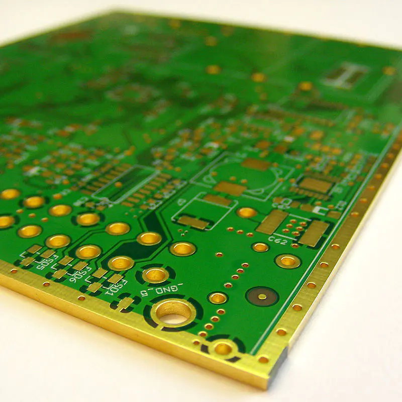
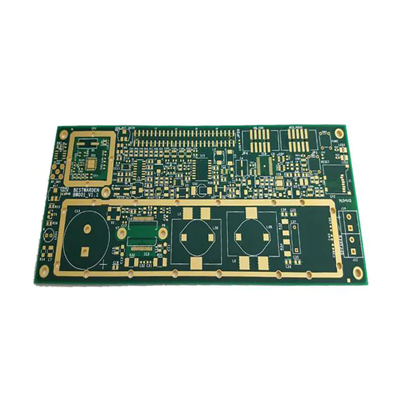
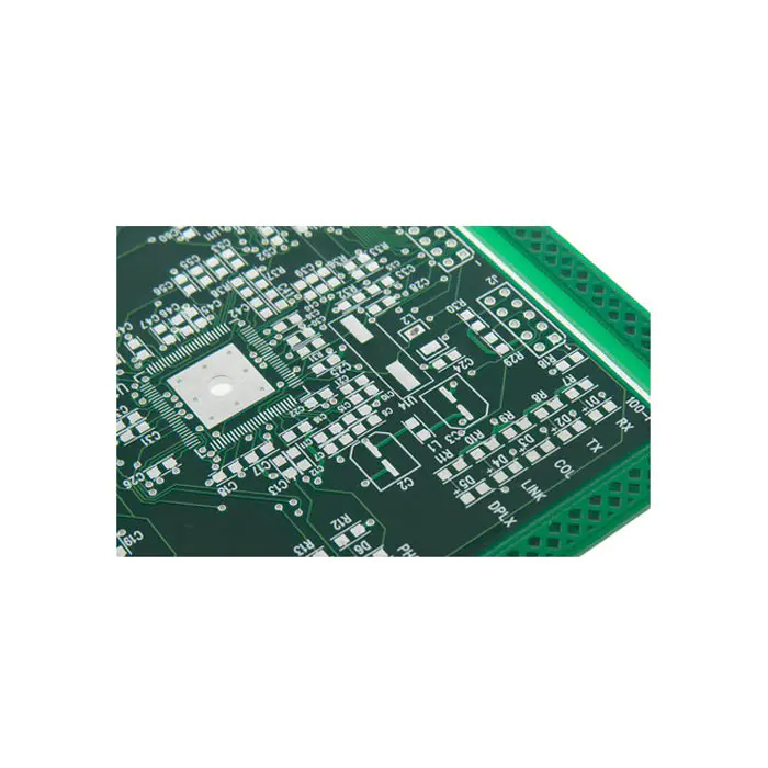
Latest products
achieving fine lines and spaces using msap: a method to form fine-line circuits on organic substrates using traditional plating equipment.
by:A-TECH
2020-01-23
Only with the progress of the design of electronic components and printed circuit boards and the manufacturing process required to reduce the size, increase the density of components and increase the speed of signals can these technical products today and tomorrow be possible to achieve, while maintaining high returns and competitive costs.
This article reviews the history subtraction printing-and-
The etching method for producing anHDI PCB and the MSAP process as a method to enhance the capability of the hdi pcb is discussed.
Traditionally, hdi pcb circuit formation is printed using subtraction-and-Etching processing.
The simplest form of this process is from the outer foil layer of about 12 to 18 [micro]
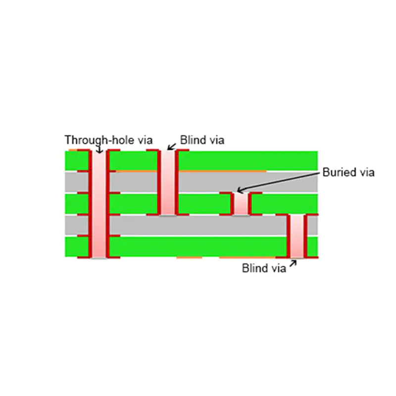
The thickness of a laser or mechanical drill into a blind hole.
Then, by plasma or chemical scale removal or a combination of the two, remove the panels to clean any resin residue on the target plate and assign some terrain to the via Wall to adhere to subsequent deposits.
The panel is then treated through major metalizing processes such as chemical copper, carbon-based direct metalization or conductive polymer to make the via Wall initially conductive, followed by flash plating of 2-4 [1]micro]
Electrolytic copper m.
After Flash plating using electrolytic copper, process the panel by filling electrolytic copper in panel plating mode.
Copper is chemically formulated by filling the solution, which can make full use of copper while minimizing the accumulation of copper on the surface.
At this step, it is usually 20 [micro]
3 Existing [m surface copper added]micro]
Flash copper m and 18 [:micro]M of copper foil.
The plating panel is then stretched and etched with a dry film to form a circuit pattern.
Bare copper (~40[micro]m)
Chemical reactions are defined using traditional copper chloride etchaway.
Then, print using traditional materials and lamination processes and subtraction-and-
Repeat Etchsequence.
General Print-and-
Etching processing is limited in terms of the minimum line width and spacing, as the etching solution tends to be etched equally in all directions.
This leads to traces of the ladder profile that, as the width of the line decreases, are detrimental to product performance (FIGURE 2).
Definition with controlled impedance and consistent line profile are critical in fine measurement
Line application.
General Print-and-
Etching treatment is usually limited to the width and spacing of about 60 to 100 [micro]
M, allows a single tracking route with pad spacing of 0. 5mm (FIGURE 3).
The further reduction of electronic equipment and the increase of functions continue to promote the progress of traditional printingand-
Etchprocessing extends the life of this process technology and extends it to finer lines, spacing, and smaller structures.
From these advances, processing technologies such
Printing and etching and advanced tent processing (ATP).
The contributing factors of these processes include improved laser drilling equipment, reduced copper thickness laminate, copper surface treatment before laser drilling, and copper plating process for filling.
Improvement of C [O. sub. 2]
Moreover, the UV laser can achieve higher continuous drilling.
Smaller size mass blind micro-pores, improved by Wall shape, will not cause lestarget pad damage even in the presence of glass straps, target pad remains lessHigh-
High-quality copper foil with reduced thickness will eventually reduce the copper etching burden during circuit formation.
The development of copper surface treatment chemistry before laser drilling improves the consistency of laser energy absorption in order to be more predictable and higher-
Quality drilling.
Progress of
Filling electrolytic copper plating provides a faster and more efficient process by filling, while minimizing the accumulation of copper on the surface, once again reducing the burden of finalcopper etching.
Finally, vertical continuous plating (VCP)
Compared with the lifting system, the equipment significantly improves the consistency and thickness distribution of the copper plating process.
Anylayer print-and-
Etching and ATP are very similar to the traditional subtraction processing (FIGURE 5).
Several important differences between these processes and traditional subtraction printingand-
Etchprocess helps reduce line width and spacing.
Plating is not used for any layer and ATPprocessing-holes.
The connection between the layer and the layer is achieved by stacking or staggered micro-channels.
This eliminates the typical requirement of 25 [micro]
The m minimum value of copper plating through the center-
Holes, which may result in the need for 30 [micro]
Copper m on the surface of the panel to meet the specifications.
In the case of no direct
Electrolytic copper chemical holes specially designed for blind micro-priority filling can be used
At the same time minimize the accumulation of copper on the surface.
Microvias up to about 100 [micro]
Diameter m and 75 [micro]
The Mdeep can reliably fill copper while limiting the surface copper thickness to about 12 [micro]m.
Under these conditions, these chemical operations eliminate the voltage potential difference between the top and depth of the micropores, and the selective adsorption of additives such as platingrate inhibitors and electroplating rate accelerators.
The result is fast bottom.
Filling micro-pores with copper and suppressing copper deposition on the surface (FIGURE 7).
The result of these changes and improvements is that from the overall copper thickness to the final etching, from about 40 [micro]
About 27 [micro]m.
This allows to reduce the width and spacing of lines to about 40 [micro]
In some cases ,[micro]
M, padpitches is 0. 4mm (FIGURE 8).
Despite the progress of printing by standard subtraction, a significant reduction in line width and spacing has been achievedand-
Etching processing, further micromation requires a thin substrate, the line width and spacing are too thin for the function of subtraction printingand-
Etching Using standard stacking materials.
The IC substrate industry has a long history of producing smaller functions and fine high
Resolution lines and spacing on inorganic substrates, such as silicon, are processed using semi-additive (SAP).
Use ultra for SAP processing-
Thin base layers of copper deposited through CVD, CVD or chemical copper deposits on the entire resubmitted surface, then laminated with photoresist resistance, imaging using direct laser imaging and electrolytic copper pattern plating.
The substrate is then stripped and the substrate is differential--orflash-
Etched into a circuit.
Although the technology is very powerful, it is expensive to use in the arena between the ages of 20 and 30. micro]
The m line width and spacing on the organic substrate.
This arena is sometimes called the basement. like panels.
In this area, ICsubstrate-
Like the manufacturing process is necessary to expand the lower capabilities
Cost organic substrates while maintaining ideal properties such as large-format, lower-
High cost organic panel and standard-
Electroplating equipment for production (FIGURE 9).
Processes developed for the manufacture of substrates
Like panel is called MSAP, or modified semi-additive treatment.
Features related to this treatment include: * 30 [line width and spacing]micro]m/30[micro]m [right arrow]20[micro]m/20 [micro]m.
* Pad distance 0. 35mm.
* Two-wire routing between pads.
* Blind Microvision between 55 and 65 years of age [micro]
Diameter m, 0. 6 to 1. 0aspect ratio.
* Consistent trajectory profile of controlled impedance. * Low-
Cost organic substrate. * Low-cost mass-production-
Able to handle.
The main concepts behind MSAP processing (FIGURE 11)
It is to minimize the accumulation of copper at each stage of the process, and the ultimate goal is to minimize the final copper required for the formation of the etchfor circuit.
This is the so-called copper budget.
Figure 12 shows the typical copper budget for several variants of the theMSAP process.
Black numbers represent copper added in various process steps, while red numbers represent copper subtraction in various surface treatments or microcuts.
Typical MSAP process (see Figure 11)
Starting with an organic substrate covering about 3 [very thin copper foil]micro]m in thickness.
In the past, very thin copper foil was not available, so a thicker foil needs to be obtained by reducing lateral etching by chemical methods.
However, with the development of technology, foil suppliers provide 1 to 5 kinds [micro]
M. MSAP handles the starting foil required for competitive pricing.
Then the Microvision tube was laser
Drilling and panel separation, or by plasma or chemical separation or combination of the two, clean any resin residue from the target liner and apply some terrain to the channel wall to adhere to subsequent deposits.
Panels are processed through primary metal processes such as chemical copper and carbon.
Based on a direct metallized or conductive polymer, make viawall initially conductive, and then do a flash plating of 2-4 [micro]
Electrolytic copper m.
In some cases, the manufacturer that makes use of electric-plating, rather than flash plating after primary metalization
Lesscopper will increase the thickness of chemical copper to about 1. 0 to 1. 2[micro]
To save the extra electrolytic copper plating, m and omit the electrolytic copper flash.
There is no filler panel in MSAP as this additional copper plating thickness must be finally etched to adversely affect fine processing
Production line tracking profile and process capability.
Panel using laser direct imaging and pattern imaging
About 18 to 20 plating [micro]m of copper.
Pattern plating is to fully fill the microchips with copper and build the copper traces to the desired height.
The progress of chemical electrolysis by filling copper improves the speed and efficiency of vibration, while minimizing the amount of copper on the surface.
At the same time, they improved the overall profile of the traces on the interior of the structure and on large panels, allowing the mass production of precise structures.
After plating, peel off the resistance and perform differential or flash to form the final circuit.
Because to control the amount of copper deposited throughout the process, there are usually only 2 to 3 [micro]
Remove the copper of m in Flash etching.
This smallest copper etching retains the outline of the circuit trace, allowing the production of finer lines (FIGURE 13).
Then, build multiple layers using pre-coding tailored for MSAPprocessing.
These pre-dip layers are much thinner to accommodate the smaller size and the need to reduce the profile of the thickness plate.
The dielectric thickness can be as low as 40 [micro]m.
They must also be in z-
The direction under the thermal offset reduces the mechanical stress placed on the plated microchip, and when the feature size is reduced, the whoseinterconnect contact area is greatly reduced.
The reduced contact area reduces the absolute load required for structural separation.
Which process to use?
The choice of whether or not to build a product using MSAP or any of the above-mentioned other processes will ultimately depend on board design, applications, and more granular requirements --
Line width and spacing balance relative to MSAP processing costs (
Equipment and Materials)
Compared with traditional subtraction printingand-etch.
Figure 14 provides an overall overview of the various processes discussed and adapted driven by line width and spacing requirements.
In general, traditional subtraction printingand-
Etching can be used for line width and spacing of about 60 [micro]m/60[micro]m.
Processing extended subtraction printing with any layer-and-
Etching to 40 PM/40 PM line width and spacing, ATP to 35 [micro]m/35[micro]m.
Further reduction in line width and spacing will facilitate MSAP processing with a capacity of as low as 20 [micro]m/20[micro]m.
Abstract: The desire to achieve greater device functionality, connectivity and speed on small portable devices at affordable prices continues to drive the renewal of electronic products, this requires a reduction in such as Microvision holes, and thickness.
Reducing line width and spacing and applications using them requires critical control of the trajectory profile for optimal performance.
Figure 15 details these reductions.
Development of Traditional subtraction printingan-
Detch process has extended this type of processing power to the line width and spacing of 35pm/35pm.
The adoption of a variety of SAP manufacturing processes commonly used in the IC substrategy industry needs to be further reduced, including LDI resistance and imaging, improved laser drilling, extremely thin copper foil plated through filling patterns, then flash etching in a process called MSAP.
Reliable costs are provided by MSAP
Effective manufacturing process for producing fine products
Use the traditional high-20 pm line width and spacing to reduce the HDI line on the organic substrate to twenty o\'clock P. M. /line
Vertical Continuous platter and other volume platter equipment.
MSAP offers high yilieldson-
Format the board to realize the control of the base plate manufacturing costlike panels.
Bibliography (English)1. )T. Rapala-Virtaner, E. Helminen and T. Jokela,\"Next-
Generation Super
PCB magazine, May 2015, challenges in the manufacture of thin PCB. (2. )M.
Gantz, \"mSAP: New PCB manufacturing for 5g smartphones is imperative\", electronic design, electronic design. com/industrial-Automation/msap-new-pcb-manufacturing-imperative-5g-smart-phones, Oct. 23, 2017. (3. )J. Rasmussen, A. Lachowicz, D. Isik and H.
Verbunt, \"Microvia filling: a challenge to process quality,\" onboard technology, April 2006.
Rich bellemare is the application manager for MacDermidEnthone electronic solutions; richard.
Bellemare @ macdermidcom.
JORDANKOLOGE is a technical marketing specialist, Medes ElectronicsSolutions; jordan.
Kologe @ madder. com.
Description: Figure 1.
Subtraction printing and etching.
Description: Figure 2.
Trace profile after etching.
Description: Figure 3.
Pad spacing and track wiring with subtraction printing-and-etch.
Description: Figure 4. Typical print-and-etch microvias.
Description: Figure 5.
Subtraction printing and etching.
Description: Figure 6.
Typical anylayer build.
Description: Figure 7.
Bottom offer-up filling.
Description: Figure 8.
Any layer of pad spacing and routing.
Description: Figure 9.
Integration of technology.
Description: Figure 10.
MSAP pad spacing and routing.
Description: Figure 11.
MSAP processing.
Description: Figure 13.
Tracking profile after MSAP processing.
Description: Figure 14.
Process capability.
Description: Figure 15.
This article reviews the history subtraction printing-and-
The etching method for producing anHDI PCB and the MSAP process as a method to enhance the capability of the hdi pcb is discussed.
Traditionally, hdi pcb circuit formation is printed using subtraction-and-Etching processing.
The simplest form of this process is from the outer foil layer of about 12 to 18 [micro]
The thickness of a laser or mechanical drill into a blind hole.
Then, by plasma or chemical scale removal or a combination of the two, remove the panels to clean any resin residue on the target plate and assign some terrain to the via Wall to adhere to subsequent deposits.
The panel is then treated through major metalizing processes such as chemical copper, carbon-based direct metalization or conductive polymer to make the via Wall initially conductive, followed by flash plating of 2-4 [1]micro]
Electrolytic copper m.
After Flash plating using electrolytic copper, process the panel by filling electrolytic copper in panel plating mode.
Copper is chemically formulated by filling the solution, which can make full use of copper while minimizing the accumulation of copper on the surface.
At this step, it is usually 20 [micro]
3 Existing [m surface copper added]micro]
Flash copper m and 18 [:micro]M of copper foil.
The plating panel is then stretched and etched with a dry film to form a circuit pattern.
Bare copper (~40[micro]m)
Chemical reactions are defined using traditional copper chloride etchaway.
Then, print using traditional materials and lamination processes and subtraction-and-
Repeat Etchsequence.
General Print-and-
Etching processing is limited in terms of the minimum line width and spacing, as the etching solution tends to be etched equally in all directions.
This leads to traces of the ladder profile that, as the width of the line decreases, are detrimental to product performance (FIGURE 2).
Definition with controlled impedance and consistent line profile are critical in fine measurement
Line application.
General Print-and-
Etching treatment is usually limited to the width and spacing of about 60 to 100 [micro]
M, allows a single tracking route with pad spacing of 0. 5mm (FIGURE 3).
The further reduction of electronic equipment and the increase of functions continue to promote the progress of traditional printingand-
Etchprocessing extends the life of this process technology and extends it to finer lines, spacing, and smaller structures.
From these advances, processing technologies such
Printing and etching and advanced tent processing (ATP).
The contributing factors of these processes include improved laser drilling equipment, reduced copper thickness laminate, copper surface treatment before laser drilling, and copper plating process for filling.
Improvement of C [O. sub. 2]
Moreover, the UV laser can achieve higher continuous drilling.
Smaller size mass blind micro-pores, improved by Wall shape, will not cause lestarget pad damage even in the presence of glass straps, target pad remains lessHigh-
High-quality copper foil with reduced thickness will eventually reduce the copper etching burden during circuit formation.
The development of copper surface treatment chemistry before laser drilling improves the consistency of laser energy absorption in order to be more predictable and higher-
Quality drilling.
Progress of
Filling electrolytic copper plating provides a faster and more efficient process by filling, while minimizing the accumulation of copper on the surface, once again reducing the burden of finalcopper etching.
Finally, vertical continuous plating (VCP)
Compared with the lifting system, the equipment significantly improves the consistency and thickness distribution of the copper plating process.
Anylayer print-and-
Etching and ATP are very similar to the traditional subtraction processing (FIGURE 5).
Several important differences between these processes and traditional subtraction printingand-
Etchprocess helps reduce line width and spacing.
Plating is not used for any layer and ATPprocessing-holes.
The connection between the layer and the layer is achieved by stacking or staggered micro-channels.
This eliminates the typical requirement of 25 [micro]
The m minimum value of copper plating through the center-
Holes, which may result in the need for 30 [micro]
Copper m on the surface of the panel to meet the specifications.
In the case of no direct
Electrolytic copper chemical holes specially designed for blind micro-priority filling can be used
At the same time minimize the accumulation of copper on the surface.
Microvias up to about 100 [micro]
Diameter m and 75 [micro]
The Mdeep can reliably fill copper while limiting the surface copper thickness to about 12 [micro]m.
Under these conditions, these chemical operations eliminate the voltage potential difference between the top and depth of the micropores, and the selective adsorption of additives such as platingrate inhibitors and electroplating rate accelerators.
The result is fast bottom.
Filling micro-pores with copper and suppressing copper deposition on the surface (FIGURE 7).
The result of these changes and improvements is that from the overall copper thickness to the final etching, from about 40 [micro]
About 27 [micro]m.
This allows to reduce the width and spacing of lines to about 40 [micro]
In some cases ,[micro]
M, padpitches is 0. 4mm (FIGURE 8).
Despite the progress of printing by standard subtraction, a significant reduction in line width and spacing has been achievedand-
Etching processing, further micromation requires a thin substrate, the line width and spacing are too thin for the function of subtraction printingand-
Etching Using standard stacking materials.
The IC substrate industry has a long history of producing smaller functions and fine high
Resolution lines and spacing on inorganic substrates, such as silicon, are processed using semi-additive (SAP).
Use ultra for SAP processing-
Thin base layers of copper deposited through CVD, CVD or chemical copper deposits on the entire resubmitted surface, then laminated with photoresist resistance, imaging using direct laser imaging and electrolytic copper pattern plating.
The substrate is then stripped and the substrate is differential--orflash-
Etched into a circuit.
Although the technology is very powerful, it is expensive to use in the arena between the ages of 20 and 30. micro]
The m line width and spacing on the organic substrate.
This arena is sometimes called the basement. like panels.
In this area, ICsubstrate-
Like the manufacturing process is necessary to expand the lower capabilities
Cost organic substrates while maintaining ideal properties such as large-format, lower-
High cost organic panel and standard-
Electroplating equipment for production (FIGURE 9).
Processes developed for the manufacture of substrates
Like panel is called MSAP, or modified semi-additive treatment.
Features related to this treatment include: * 30 [line width and spacing]micro]m/30[micro]m [right arrow]20[micro]m/20 [micro]m.
* Pad distance 0. 35mm.
* Two-wire routing between pads.
* Blind Microvision between 55 and 65 years of age [micro]
Diameter m, 0. 6 to 1. 0aspect ratio.
* Consistent trajectory profile of controlled impedance. * Low-
Cost organic substrate. * Low-cost mass-production-
Able to handle.
The main concepts behind MSAP processing (FIGURE 11)
It is to minimize the accumulation of copper at each stage of the process, and the ultimate goal is to minimize the final copper required for the formation of the etchfor circuit.
This is the so-called copper budget.
Figure 12 shows the typical copper budget for several variants of the theMSAP process.
Black numbers represent copper added in various process steps, while red numbers represent copper subtraction in various surface treatments or microcuts.
Typical MSAP process (see Figure 11)
Starting with an organic substrate covering about 3 [very thin copper foil]micro]m in thickness.
In the past, very thin copper foil was not available, so a thicker foil needs to be obtained by reducing lateral etching by chemical methods.
However, with the development of technology, foil suppliers provide 1 to 5 kinds [micro]
M. MSAP handles the starting foil required for competitive pricing.
Then the Microvision tube was laser
Drilling and panel separation, or by plasma or chemical separation or combination of the two, clean any resin residue from the target liner and apply some terrain to the channel wall to adhere to subsequent deposits.
Panels are processed through primary metal processes such as chemical copper and carbon.
Based on a direct metallized or conductive polymer, make viawall initially conductive, and then do a flash plating of 2-4 [micro]
Electrolytic copper m.
In some cases, the manufacturer that makes use of electric-plating, rather than flash plating after primary metalization
Lesscopper will increase the thickness of chemical copper to about 1. 0 to 1. 2[micro]
To save the extra electrolytic copper plating, m and omit the electrolytic copper flash.
There is no filler panel in MSAP as this additional copper plating thickness must be finally etched to adversely affect fine processing
Production line tracking profile and process capability.
Panel using laser direct imaging and pattern imaging
About 18 to 20 plating [micro]m of copper.
Pattern plating is to fully fill the microchips with copper and build the copper traces to the desired height.
The progress of chemical electrolysis by filling copper improves the speed and efficiency of vibration, while minimizing the amount of copper on the surface.
At the same time, they improved the overall profile of the traces on the interior of the structure and on large panels, allowing the mass production of precise structures.
After plating, peel off the resistance and perform differential or flash to form the final circuit.
Because to control the amount of copper deposited throughout the process, there are usually only 2 to 3 [micro]
Remove the copper of m in Flash etching.
This smallest copper etching retains the outline of the circuit trace, allowing the production of finer lines (FIGURE 13).
Then, build multiple layers using pre-coding tailored for MSAPprocessing.
These pre-dip layers are much thinner to accommodate the smaller size and the need to reduce the profile of the thickness plate.
The dielectric thickness can be as low as 40 [micro]m.
They must also be in z-
The direction under the thermal offset reduces the mechanical stress placed on the plated microchip, and when the feature size is reduced, the whoseinterconnect contact area is greatly reduced.
The reduced contact area reduces the absolute load required for structural separation.
Which process to use?
The choice of whether or not to build a product using MSAP or any of the above-mentioned other processes will ultimately depend on board design, applications, and more granular requirements --
Line width and spacing balance relative to MSAP processing costs (
Equipment and Materials)
Compared with traditional subtraction printingand-etch.
Figure 14 provides an overall overview of the various processes discussed and adapted driven by line width and spacing requirements.
In general, traditional subtraction printingand-
Etching can be used for line width and spacing of about 60 [micro]m/60[micro]m.
Processing extended subtraction printing with any layer-and-
Etching to 40 PM/40 PM line width and spacing, ATP to 35 [micro]m/35[micro]m.
Further reduction in line width and spacing will facilitate MSAP processing with a capacity of as low as 20 [micro]m/20[micro]m.
Abstract: The desire to achieve greater device functionality, connectivity and speed on small portable devices at affordable prices continues to drive the renewal of electronic products, this requires a reduction in such as Microvision holes, and thickness.
Reducing line width and spacing and applications using them requires critical control of the trajectory profile for optimal performance.
Figure 15 details these reductions.
Development of Traditional subtraction printingan-
Detch process has extended this type of processing power to the line width and spacing of 35pm/35pm.
The adoption of a variety of SAP manufacturing processes commonly used in the IC substrategy industry needs to be further reduced, including LDI resistance and imaging, improved laser drilling, extremely thin copper foil plated through filling patterns, then flash etching in a process called MSAP.
Reliable costs are provided by MSAP
Effective manufacturing process for producing fine products
Use the traditional high-20 pm line width and spacing to reduce the HDI line on the organic substrate to twenty o\'clock P. M. /line
Vertical Continuous platter and other volume platter equipment.
MSAP offers high yilieldson-
Format the board to realize the control of the base plate manufacturing costlike panels.
Bibliography (English)1. )T. Rapala-Virtaner, E. Helminen and T. Jokela,\"Next-
Generation Super
PCB magazine, May 2015, challenges in the manufacture of thin PCB. (2. )M.
Gantz, \"mSAP: New PCB manufacturing for 5g smartphones is imperative\", electronic design, electronic design. com/industrial-Automation/msap-new-pcb-manufacturing-imperative-5g-smart-phones, Oct. 23, 2017. (3. )J. Rasmussen, A. Lachowicz, D. Isik and H.
Verbunt, \"Microvia filling: a challenge to process quality,\" onboard technology, April 2006.
Rich bellemare is the application manager for MacDermidEnthone electronic solutions; richard.
Bellemare @ macdermidcom.
JORDANKOLOGE is a technical marketing specialist, Medes ElectronicsSolutions; jordan.
Kologe @ madder. com.
Description: Figure 1.
Subtraction printing and etching.
Description: Figure 2.
Trace profile after etching.
Description: Figure 3.
Pad spacing and track wiring with subtraction printing-and-etch.
Description: Figure 4. Typical print-and-etch microvias.
Description: Figure 5.
Subtraction printing and etching.
Description: Figure 6.
Typical anylayer build.
Description: Figure 7.
Bottom offer-up filling.
Description: Figure 8.
Any layer of pad spacing and routing.
Description: Figure 9.
Integration of technology.
Description: Figure 10.
MSAP pad spacing and routing.
Description: Figure 11.
MSAP processing.
Description: Figure 13.
Tracking profile after MSAP processing.
Description: Figure 14.
Process capability.
Description: Figure 15.
Custom message