loading

A-TECH  >  AI - Page Sitemap  >  A-TECH tin pcb surface finish cheapest factory price for wholesale
A-TECH tin pcb surface finish cheapest factory price for wholesale

A-TECH tin pcb surface finish cheapest factory price for wholesale

Thickness
10-50um
RoHS Compliant
Yes
Additional Cost
Yes
Supply Capacity
5000 ㎡/Month
Certifications
UL, ISO9001, TS16949
Payment Terms
T/T, Paypal, WU etc.
Shipment Terms
EXW, FOB, DDU etc.
Test Way
100% E-Test
Standard
IPC CLASS 2 / CLASS 3
Price
Get Latest Price
Get the latest price
Quantity Needed:
Pieces
E-mail:
Application Scope
With wide application, Multilayer PCB can be used in the following aspects.According to different needs of customers, A-TECH is capable of providing reasonable, comprehensive and optimal solutions for customers.
Company Advantages
1. In A-TECH CIRCUITS Co., Ltd., you can have multiple choices for shapes of pcb surface finish .
2. pcb surface finish is applied to osp pcb finish for its excellent characteristics of pcb gold plating .
3. A-TECH CIRCUITS Co., Ltd. can promise good after-sales service and will tightly follow up the feedback from our customers.
4. A-TECH CIRCUITS Co., Ltd. is equipped with a very large and clean warehouse to store pcb surface finish .


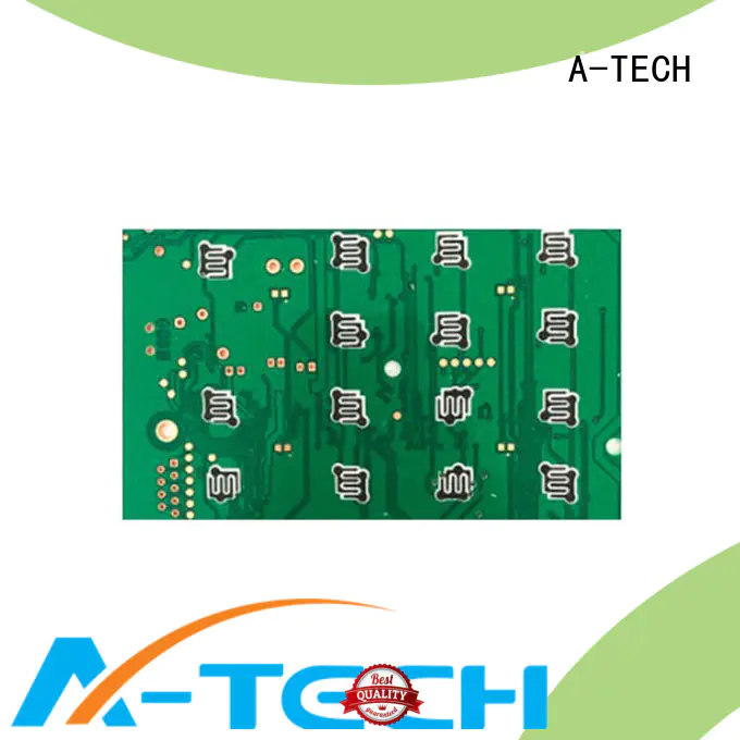
Carbon Ink is typically used to create a protective contact surface for switches, sometimes few copper elements or patterns of the PCB board are used for keyboard contacts, LCD contacts and jumpers etc, to do this it’s usable to print some conductive/resistive carbon ink over those copper part, which normally are SMD pads or fingers or other typical contact patterns.

Carbon Ink printing process is screen printing like silk screen process, the carbon ink is printed in the specified location of the PCB, after oven cured and tested, formed a carbon film which with certain resistance to instead of the original resistance components. The difference is that silkscreen is only played a welding role but carbon ink has conductive performance.

The typical thickness of carbon ink is 10-50um, because the carbon ink has good electrical conductivity, so the carbon printed on the finished PCB should have a certain gap to ensure that no short circuits, usually require the min 8mil gap for Hoz copper and min 12mil gap for 1-3oz copper, and the minimum carbon line width is 12mil.

A-TECH is a capable PCB manufacturer to offer Carbon ink process, we require the data files to clearly indicate on which side of the PCB carbon is to be applied and the carbon areas must be properly indicated on specific layers with proper file naming.


Company Features
1. A-TECH CIRCUITS Co., Ltd. has been dedicated to the pcb surface finish industry for many decades.
2. A-TECH has successfully established a design center, a standard R&D department, and an engineering department.
3. Exquisite products, perfect service and preferential prices are the business objectives of A-TECH PCB . Inquiry! Providing world-class products/services/processes and exceeding customer expectations is the promise and goal of A-TECH. Inquiry! With the support of professional team, A-TECH has won much recognition. Inquiry!
A-TECH osp pcb finish has been carefully inspected. It has passed the checks on obvious damage or defects in the accessories, connectors, plugs or extension outlet sockets. It offers exceptional reproduction of colors
The quality of A-TECH pcb surface finish meets both domestic and international standards for sanitary ware. It will be scrutinized for its chemical properties and hygiene level by the QC department. It can be customized to fit different model numbers of devices
The base fabrics of A-TECH osp pcb finish use the highest-quality extra long staple cotton, which can be optimized for softness while maintaining lifetime durability and longevity. It is often used to replace the damaged, cracked, shattered screen or the ones with display problems
A-TECH pcb gold plating meets various requirements stipulated in compulsory certifications. They are mainly domestic standards CCC and overseas standards such as BSI, PSE, SAA, UL, and CE. The product does not have problems like dead touch and slow respond touch
A-TECH pcb gold plating is produced using a wide range of high-tech equipment. It will be processed under the pressing machine, high-frequency pinching machine, and electrostatic spraying machine which all feature high automation level. It has the same thickness as the original ones
The product has a fine melting point. It is an optimized refractory material which can prevent it have a reaction with the molten materials. Full view is one of the biggest selling points of this product
Product Message
Chat Online 编辑模式下无法使用
Chat Online inputting...
Please hold on and we will get back to you soon