

Related Products


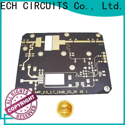
Microwave RF PCB, it’s also known as high frequent PCB, they use materials of excellent dielectric property for its main body with other dielectric materials and metal substrates matched to complete corresponding multi-layer processing or thick-film processing and manufacture and to achieve the transmission functions of excellent high thermal conductivity, low dielectric constant, high frequency and high speed.
The features of Microwave RF PCB
● The thermal expansivity should be the same with copper foil as much as possible, because the difference will lead toe copper foil separated in the changes of cold and heat.
● Heat resisting property, chemistry resisting, impact endurance, peel off resisting must be good.
● Water absorptivity must be low, high water absorptivity will affect DK and DF when in the wet environment
● DK should be small and stable enough, usually the smaller the better, high DK may lead to signal transmission delay
● DF should be small, which mainly affect quality of signal transmission, the smaller DF could make smaller signal wastage accordingly
The applications of Microwave RF PCB
● Microwave transmission
● Automobile telephone
● Wireless networks
● Wireless communications
● Satellite microwave communications
● 4G & 5G networks
A-TECH CIRCUITS have increased investment and intensity of research & development on Microwave high frequency PCB over the last few years to meet the continuously increasing demands. We have obtained rich knowledge and experience in professional manufacturing of various high-frequency PCBs from prototypes to production run. For main RF PCBs, such as Teflon PCB, Rogers PCB, Taconic PCB and Arlon PCB, we have sufficient inventory to ensure fast delivery.
| General specification for Microwave/RF PCB in A-TECH | |
| Layer Count | 1-6 |
| Board thickness | 0.4-3.2mm |
| Copper thickness | 0.5-3oz |
| Dielectric Constant(DK) | 2.2-10.3 |
| Min trace width/spacing | 4/4mil |
| Min drill hole size | 0.2mm |
| Surface treatment | HAL(Lead free), Immersion Gold/Tin/Silver, OSP, Gold Plating. |
| Material available | Teflon, Rogers, Taconic, Arlon, etc |
General inquiries & Customer Service
Tel: 86-755-2335 9039 | Fax: 86-755-3318 0939
E-Mail: Enquiry@atechcircuit.com
Skype: atechcircuits

Headquarters: 602, Building B3, Zhimei Huizhi Industrial Park, Fuyong Street, Bao'an District, Shenzhen City, China
Copyright © 2025 A-TECH CIRCUITS Co., Ltd. | All Rights Reserved
Hello, please leave your name and email here before chat online so that we won't miss your message and contact you smoothly.

