

Related Products


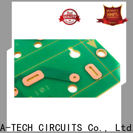
OSP, the full name is Organic Solderability Preservative, it preserves the copper surface from oxidation by applying a very thin protective layer of material over the exposed copper usually using a conveyorized process. It uses a water-based organic compound that selectively bonds to copper and provides an organometallic layer that protects the copper prior to soldering. It’s also extremely green environmentally in comparison with the other common lead free finishes, which Suffer from either being more toxic or substantially higher energy consumption.
The typical thickness of OSP is 0.2 – 0.65um and the shelf life is 6 months. It’s a simple manufacturing process to make OSP, and like HASL finish, the production cost of OSP is lower than most of other surface finishes.
The advantages of OSP
● Cost effective / Low cost
● Simple process
● Excellent flatness
● Re-workable
● Clean, environmentally friendly process
The disadvantages of OSP
● Short shelf life
● Very sensitive to handling – gloves must be used and scratches avoided
● Short operating window between assembly stages
● Not suitable for multiple soldering processes
● Difficult to inspect or measure thickness
A-TECH own OSP line in house, it’s nowadays mainly used to build single-sided FR4 PCB or aluminum PCB with low cost requirements.
General inquiries & Customer Service
Tel: 86-755-2335 9039 | Fax: 86-755-3318 0939
E-Mail: Enquiry@atechcircuit.com
Skype: atechcircuits

Headquarters: 602, Building B3, Zhimei Huizhi Industrial Park, Fuyong Street, Bao'an District, Shenzhen City, China
Copyright © 2025 A-TECH CIRCUITS Co., Ltd. | All Rights Reserved
Hello, please leave your name and email here before chat online so that we won't miss your message and contact you smoothly.

