loading

A-TECH  >  AI - Page Sitemap  >  A-TECH free pcb surface finish free delivery at discount
A-TECH free pcb surface finish free delivery at discount

A-TECH free pcb surface finish free delivery at discount

Thickness
1-40um
Shelf Life
12 Months
Solderability
Good
RoHS Compliant
Yes
Additional Cost
No
Supply Capacity
20000 ㎡/Month
Certifications
UL, ISO9001, TS16949
Payment Terms
T/T, Paypal, WU etc.
Shipment Terms
EXW, FOB, DDU etc.
Test Way
100% E-Test
Standard
IPC CLASS 2 / CLASS 3
Price
Get Latest Price
Get the latest price
Quantity Needed:
Pieces
E-mail:


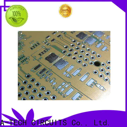
HAL(Lead Free), the full name is Hot Air leveling with Lead Free. Compared with HASL, the main difference for HAL(Lead Free) is the element of material which do not contain Lead(Pb), so it’s RoHS Compliant and it’s much more popular and widely used in PCB manufacturing.

HAL(Lead Free) requires higher run temperatures for lead free solder and longer contact time, the production cost for HAL(Lead Free) is slightly higher than HASL(Tin/Lead).

The manufacturing process of HAL(Lead Free) is similar to HASL(Tin/Lead), the circuit boards will be submersed in molten solder(Lead Free). This solder will cover all the exposed copper surfaces. Upon retraction from the solder, high pressure hot air is blown over the surface through air knives, this levels the solder deposit and removes the excess solder from the surface of printed circuit boards.

The typical thickness of HAL(Lead Free) is 1-40um and the shelf life is 12 months.


The advantages of HAL(Lead Free) surface finish

● Good solderability / wettability
● RoHS Compliant
● Good reflow properties
● Large processing window is allowed
● Multiple thermal excursions
● Can be widely used


The disadvantages of HAL(Lead Free) surface finish

● Uneven surface
● Not suitable for PCBs with fine pitch
● Thermal shock
● Solder bridge
● Plugged or Reduced plated through holes


A-TECH have HAL(Lead Free) surface finish in house, It’s basically the highest proportion of finish used for circuit boards without fine pitch or high density layout. We don’t have any additional cost for HAL(Lead Free) surface finish.


The materials of A-TECH pcb surface finish are strictly selected and their quality reaches the international packaging standards, which helps this product withstand the test of the time. Its packaging can be customized per customers' specifications
A-TECH immersion tin pcb finish is developed by our in-house structural engineering team who is dedicated to designing packaging that can bring customers vision and ideas into reality. This product is easy to clean and can be used many times
A-TECH immersion tin pcb finish is carried out by adopting the packaging and printing method which is flexible in its use of color and has the capacity to print on a vast array of materials. This product is designed to make users feel more comfortable in the course of the teeth whitening process
The production technology of A-TECH pcb surface finish is constantly updated. Thanks to the adoption of high technology, its packaging capacity is ensured. This product comes in a variety of volumes
The design of A-TECH pcb surface finish is carried out by a team of designers who adopt innovative concepts of its colors, fonts, and shapes. This product is effective in eliminating extrinsic staining
The product is strong enough to protect goods from environmental and physical hazards that this prodcut will be faced with during transport and storage. This product comes in a variety of volumes
Product Message
Chat Online 编辑模式下无法使用
Chat Online inputting...
Please hold on and we will get back to you soon